

Memory Module and Method of Manufacturing the Same
- Summary
- Abstract
- Description
- Claims
- Application Information
AI Technical Summary
Benefits of technology
Problems solved by technology
Method used
Image

Examples
Embodiment Construction
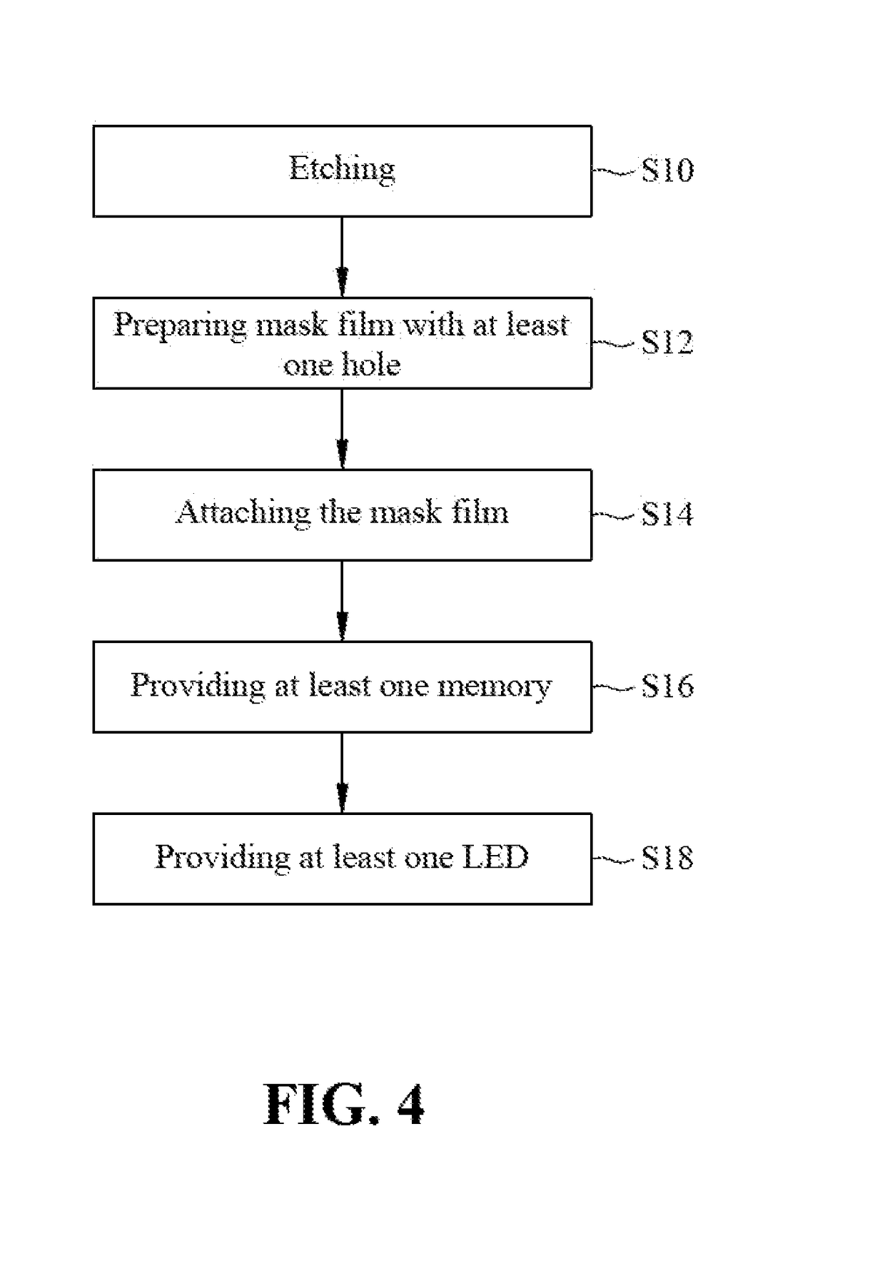
[0024]The accompanying drawings are included to provide a further understanding of the invention, and are incorporated in and constitute a part of this specification. The drawings illustrate embodiments of the invention and, together with the description, serve to explain the principles of the invention.
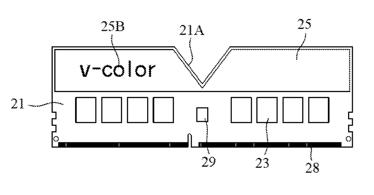
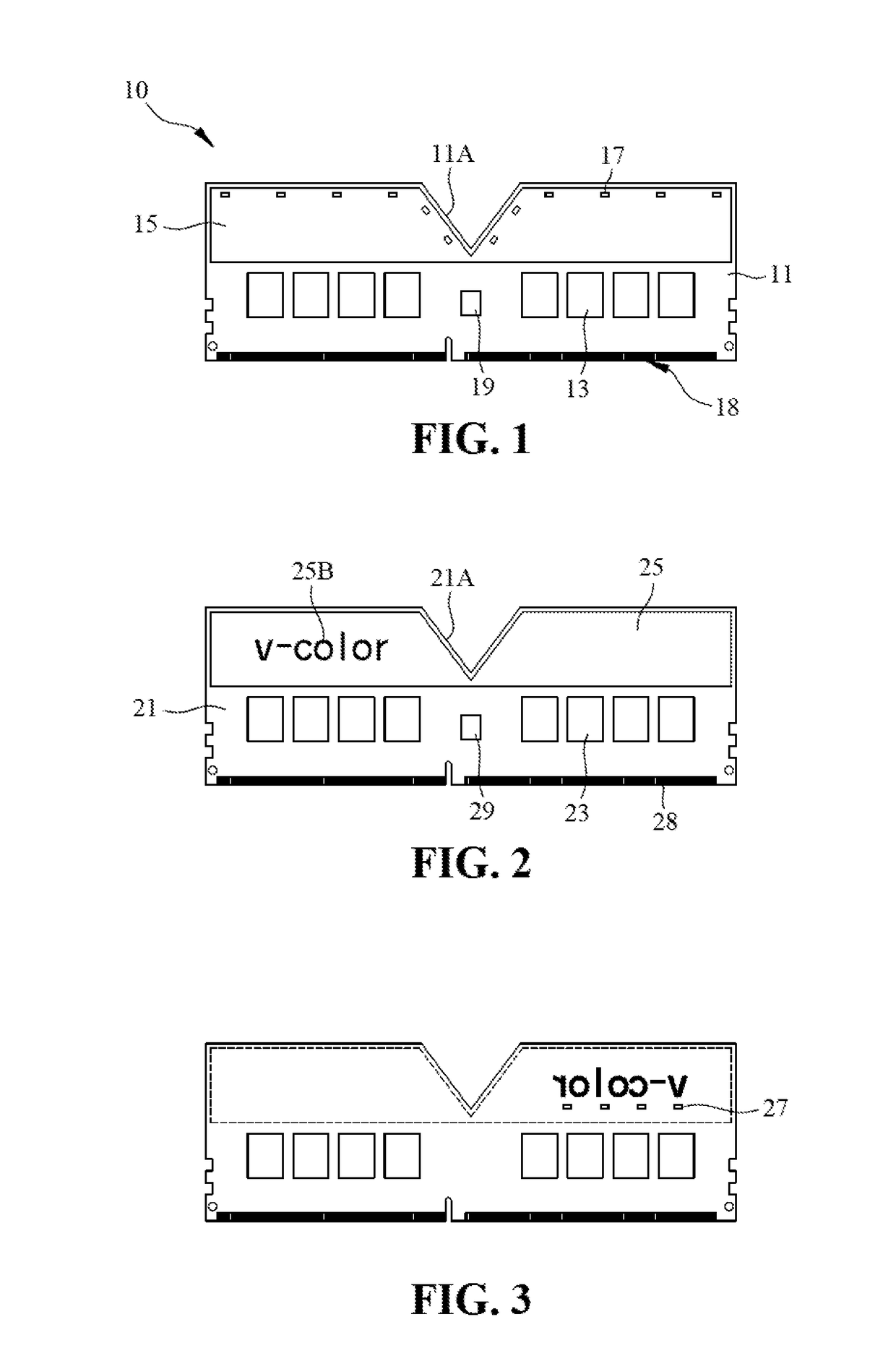
[0025]Please refer to FIG. 1 illustrating the memory module according to the first embodiment of the present invention. As shown in FIG. 1, the memory module 10 of the first embodiment generally comprises a substrate 11, at least one memory 13, a mask film 15 and at least one light emitting diode (LED) 17. The substrate 11 is at least partially transparent, possesses electrical insulation and comprises electrical circuit (not shown). The mask film 15 is opaque, preferably formed of copper foil by the etching process, and provided on the substrate 11 and close to the upper rim of the substrate 11. The at least one memory 13 and the at least one LED 17 are configured on the substrate 1...
PUM
 Abstract
Description
Claims
Application Information