Electrostatic discharge protection circuit

a protection circuit and electrostatic discharge technology, applied in the direction of diodes, circuit arrangements, semiconductor devices, etc., can solve the problems of inability to protect the internal circuit, easy latched up, and esd may destroy semiconductor devices, so as to save the layout area

Active Publication Date: 2017-07-27
UNITED MICROELECTRONICS CORP
View PDF5 Cites 3 Cited by
  • Summary
  • Abstract
  • Description
  • Claims
  • Application Information

AI Technical Summary

Benefits of technology

[0007]It is an objective of the present invention is to provide an electrostatic discharge protection circuit and an electrostatic discharge protection device to increase the holding voltage and save the layout area.
[0011]In the ESD protection circuit and the ESD protection device of the present invention, the holding voltage is increased only by adjusting the base width of the BJT. Thus, the ESD protection device doesn't require extra layout area to dispose extra transistors. Therefore, the ESD protection device not only solves the latch-up issue but also saves the layout area.

Problems solved by technology

ESD may destroy semiconductor devices because the rapid discharge can produce a relatively large current.
Since that, when the traditional ESD protection circuit is triggered on, it is easily latched up and cannot protect the internal circuit.

Method used


Image

  • Electrostatic discharge protection circuit
  • Electrostatic discharge protection circuit
  • Electrostatic discharge protection circuit

Examples


Embodiment Construction

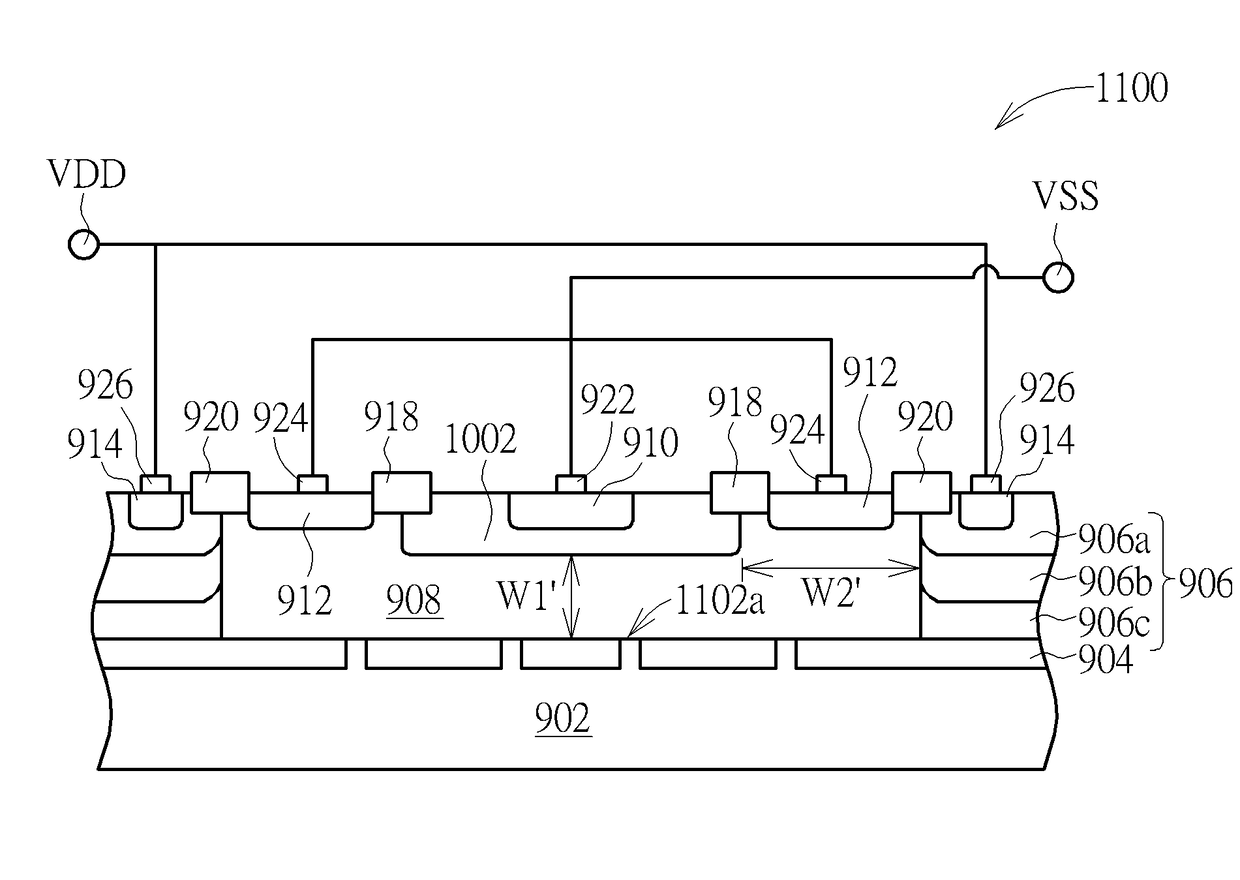
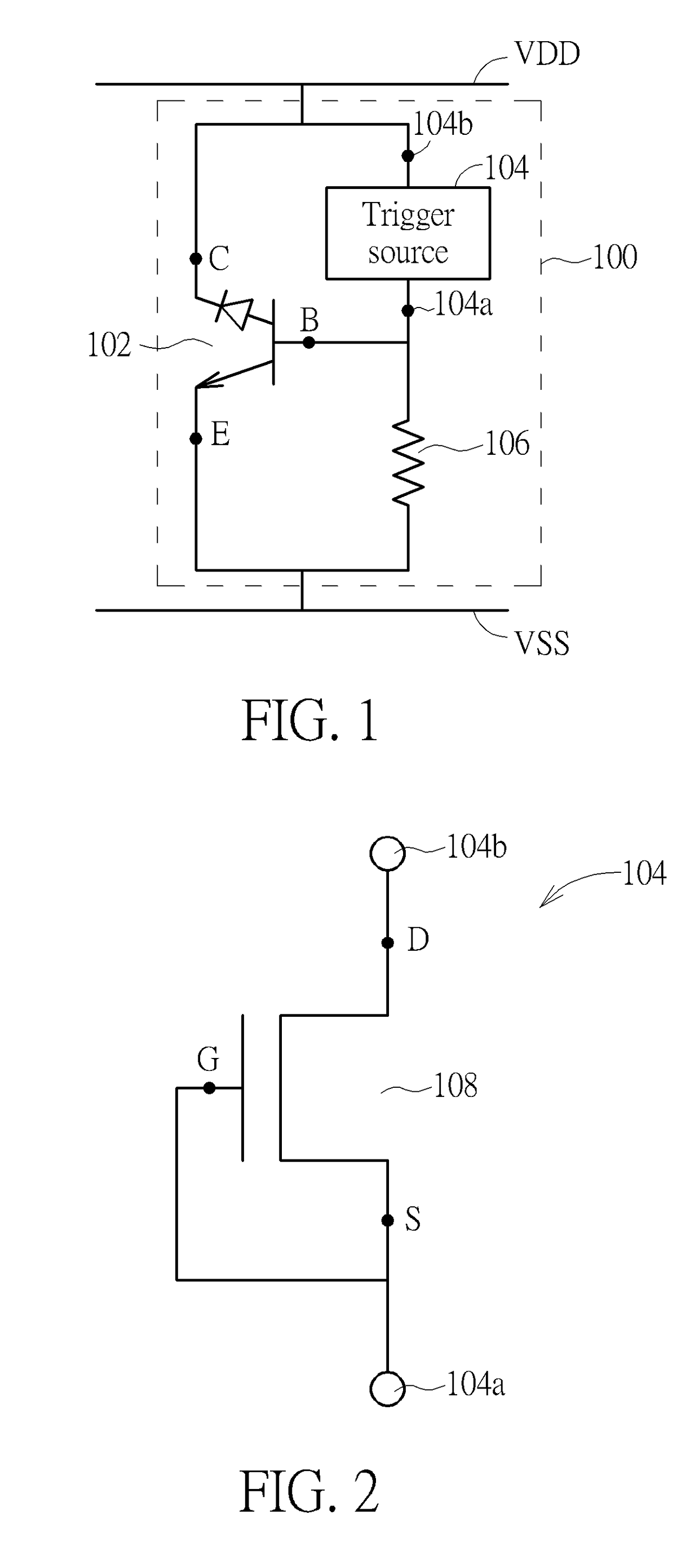
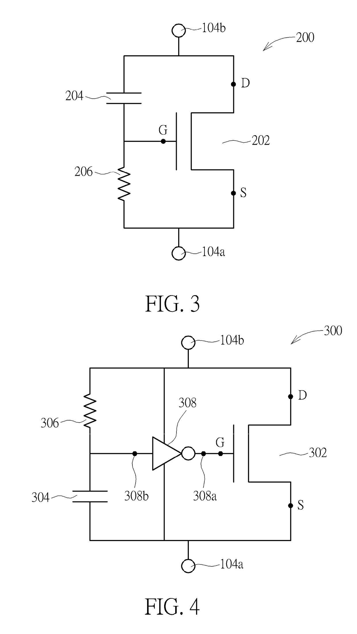
[0026]Refer to FIG. 1, which is a schematic diagram illustrating an ESD protection circuit according to a first embodiment of the present invention. As shown in FIG. 1, the ESD protection circuit 100 is electrically connected between a terminal for generating the electrostatic charges and another terminal for releasing the ESD current. In this embodiment, the ESD protection circuit 100 may be electrically connected between a high voltage power line VDD and a low voltage power line VSS and used as a power-rail ESD clamp circuit, so that the ESD protection circuit 100 may be used to protect an internal circuit electrically connected between the high voltage power line VDD and the low voltage power line VSS from being damaged by an ESD event occurring in the high voltage power line VDD. The present invention is not limited to this.

[0027]In this embodiment, the ESD protection circuit 100 includes a bipolar junction transistor (BJT) 102 and a trigger source 104. The BJT 102 may include a...


PUM


Abstract

The present invention provides an ESD protection circuit electrically connected between a high voltage power line and a low voltage power line, and the ESD protection circuit includes a bipolar junction transistor (BJT) and a trigger source. A collector of the BJT is electrically connected to the high voltage power line, and an emitter and a base of the BJT are electrically connected to the low voltage power line. The trigger source is electrically connected between the base of the BJT and the high voltage power line.

Description

CROSS REFERENCE TO RELATED APPLICATIONS[0001]This application is a divisional application of and claims the benefit of U.S. patent application Ser. No. 14 / 594,173, filed Jan. 12, 2015.BACKGROUND OF THE INVENTION[0002]1. Field of the Invention[0003]The present invention relates to an electrostatic discharge (ESD) protection circuit and an ESD protection device, and more particularly, to an ESD protection circuit and an ESD protection device using a trigger source to trigger a bipolar junction transistor to protect a circuit during an ESD event.[0004]2. Description of the Prior Art[0005]Electrostatic Discharge (ESD) is a rapid discharge that flows between two objects due to the built-up of static charge. ESD may destroy semiconductor devices because the rapid discharge can produce a relatively large current. In order to reduce the semiconductor failures due to ESD, ESD protection circuits have been developed to provide a current discharge path. When an ESD event occurs, the discharge ...

Claims


Application Information

Patent Timeline
Patent Type & Authority Applications(United States)
IPC IPC(8): H01L27/02
CPCH01L27/0259H01L27/0288H01L27/0255H02H9/046
Inventor WANG, LI-CIHCHEN, LU-ANTANG, TIEN-HAO
Owner UNITED MICROELECTRONICS CORP
Why Eureka
Try Eureka