Three-end compact and compound SCR device for whole-chip ESD protection

A composite, full-chip technology, applied in the field of electronics, can solve the problems of large chip area, chip area loss, occupation, etc., and achieve the effect of reducing trigger voltage, reducing ESD current, and small area

Active Publication Date: 2019-08-30
UNIV OF ELECTRONICS SCI & TECH OF CHINA
View PDF5 Cites 7 Cited by
  • Summary
  • Abstract
  • Description
  • Claims
  • Application Information

AI Technical Summary

Problems solved by technology

[0005] In the full-chip ESD protection circuit, a single device is required between IO and VDD and VSS as an ESD protection device, which occupies a large chip area. In addition, in order to quickly discharge the ESD current under ESD stress conditions, it is necessary to An effective ESD clamp circuit is repeatedly inserted between the VDD and VSS supply lines at a suitable distance to provide a low impedance path between the VDD and VSS supply lines, which also consumes a lot of chip area

Method used


Image

  • Three-end compact and compound SCR device for whole-chip ESD protection
  • Three-end compact and compound SCR device for whole-chip ESD protection
  • Three-end compact and compound SCR device for whole-chip ESD protection

Examples


Embodiment Construction

[0023] The present invention will be described in detail below in conjunction with the accompanying drawings and specific embodiments.

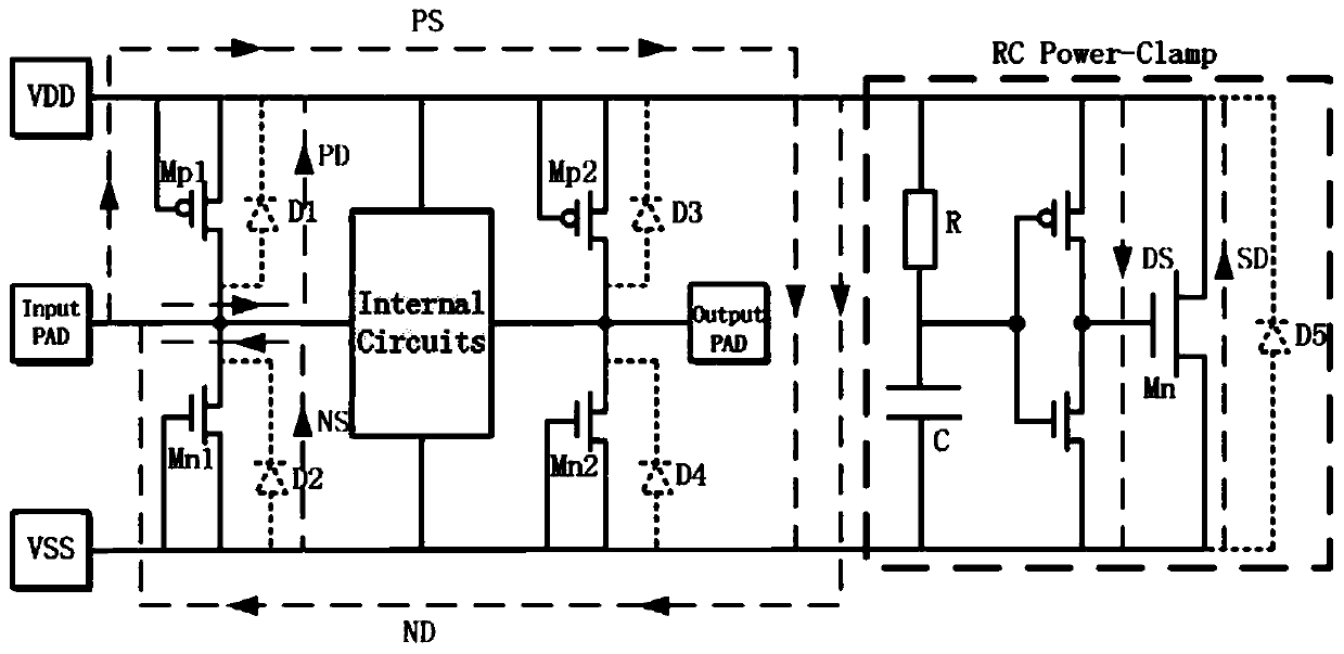
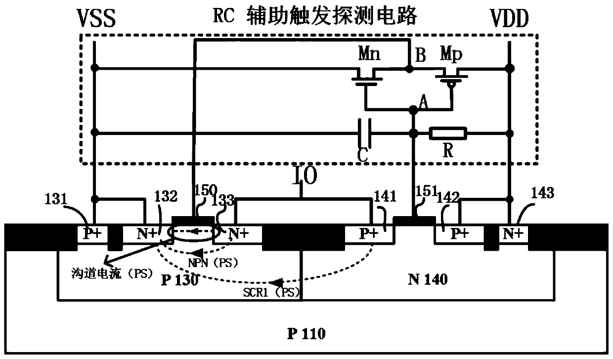
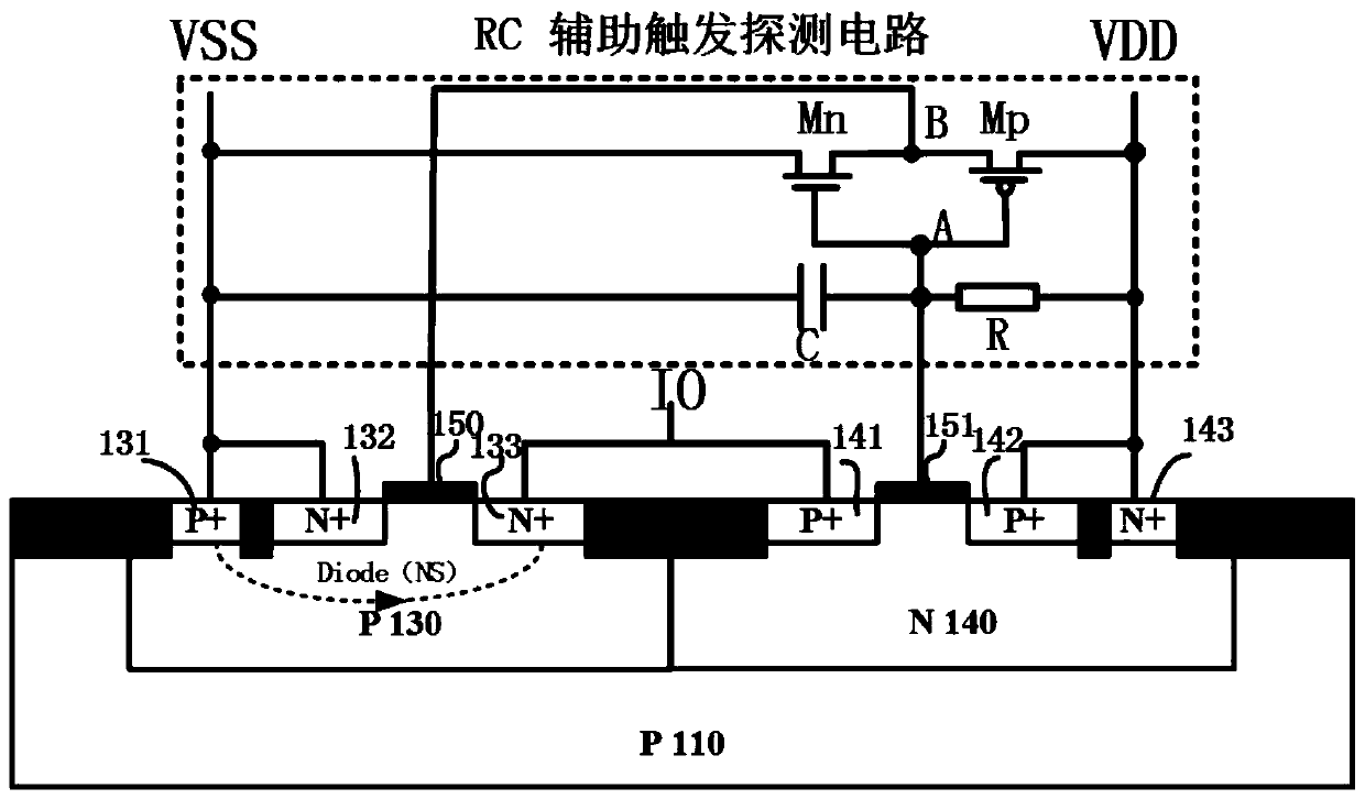
[0024] This embodiment provides a three-terminal compact composite SCR device for full-chip ESD protection, such as Figure 2 to Figure 7 shown; including: a main discharge CCSCR device and an RC auxiliary trigger detection circuit; where,

[0025] The main discharge CCSCR device includes:

[0026]p-type silicon substrate 110; the well region formed on the p-type substrate 110, the well region includes a p-type well region 130 and an n-type well region 140, the two well regions are adjacent; the p A p-type heavily doped region 131, an n-type heavily doped region 132, and an n-type heavily doped region 133 are provided in the well region 130; a p-type heavily doped region 140 is provided in the n-type well region region 141, a p-type heavily doped region 142 and an n-type heavily doped region 143; a gate oxide layer is arranged on the silico...


PUM


Abstract

The present invention belongs to the technical field of electrons, especially relates to the design of an ESD (Electro-Static discharge) protection circuit, and especially provides a three-end compactand compound SCR device (CCSCR) for whole-chip ESD protection. The three-end compact and compound SCR device comprises a main discharge CCSCR and a RC auxiliary trigger detection circuit; the main discharge CCSCR is a three-end device, three parasitic SCR pathways are introduced on the basis of the CMOS device structure so that the whole-chip ESD protection with high robustness is achieved in a smaller territory area; the RC auxiliary trigger detection circuit is introduced to further reduce the triggering voltage of the device; and besides, the CCSCR can be taken as a two-end device to supply ESD protection between any one IO port and a power supply.

Description

technical field [0001] The invention belongs to the field of electronic technology, and in particular relates to the design of an electrostatic discharge (Electro-Static discharge, ESD for short) protection circuit, especially a silicon controlled rectifier SCR (Silicon Controlled Rectifier for short SCR) used for full-chip ESD protection. Background technique [0002] In the process of semiconductor chip manufacturing, packaging and transportation, and user use, ESD phenomena are ubiquitous; the instantaneous high-voltage electrostatic pulse generated by ESD can flow into the chip through the pins of the chip, causing gate oxide breakdown and damage to the internal circuit of the chip. unable to work properly. In recent years, with the rapid development of the electronics industry, the line width of integrated circuits has been further reduced, the integration level of chips has been further increased, and the gate oxide layer of MOSFET devices has become thinner and thinne...

Claims


Application Information

Patent Timeline
Patent Type & Authority Applications(China)
IPC IPC(8): H01L27/02
CPCH01L27/0248H01L27/0266
Inventor 刘志伟董小雨刘继芝
Owner UNIV OF ELECTRONICS SCI & TECH OF CHINA
Why Eureka
Try Eureka