Bidirectional silicon-controlled electrostatic protection device with high protection level and fabrication method thereof

An electrostatic protection device, high protection technology, applied in the field of high-level bidirectional thyristor electrostatic protection devices and its production, can solve the problems of easily exceeding the design window, reducing the robustness of the device, and easily causing latch-up, etc., to reduce the layout area , Improve the robustness, the effect of low protection level

Active Publication Date: 2018-11-13
XIANGTAN UNIV
View PDF3 Cites 9 Cited by
  • Summary
  • Abstract
  • Description
  • Claims
  • Application Information

AI Technical Summary

Problems solved by technology

However, SCR has a high trigger voltage and low sustain voltage, which is easy to exceed the design window and cause latch-up, so it is necessary to increase its sustain voltage
However, the method of increasing the maintenance voltage will reduce the robustness of the device, so it is also necessary to consider its robustness

Method used


Image

  • Bidirectional silicon-controlled electrostatic protection device with high protection level and fabrication method thereof
  • Bidirectional silicon-controlled electrostatic protection device with high protection level and fabrication method thereof
  • Bidirectional silicon-controlled electrostatic protection device with high protection level and fabrication method thereof

Examples


Embodiment Construction

[0033] The present invention will be further described below in conjunction with the accompanying drawings and embodiments.

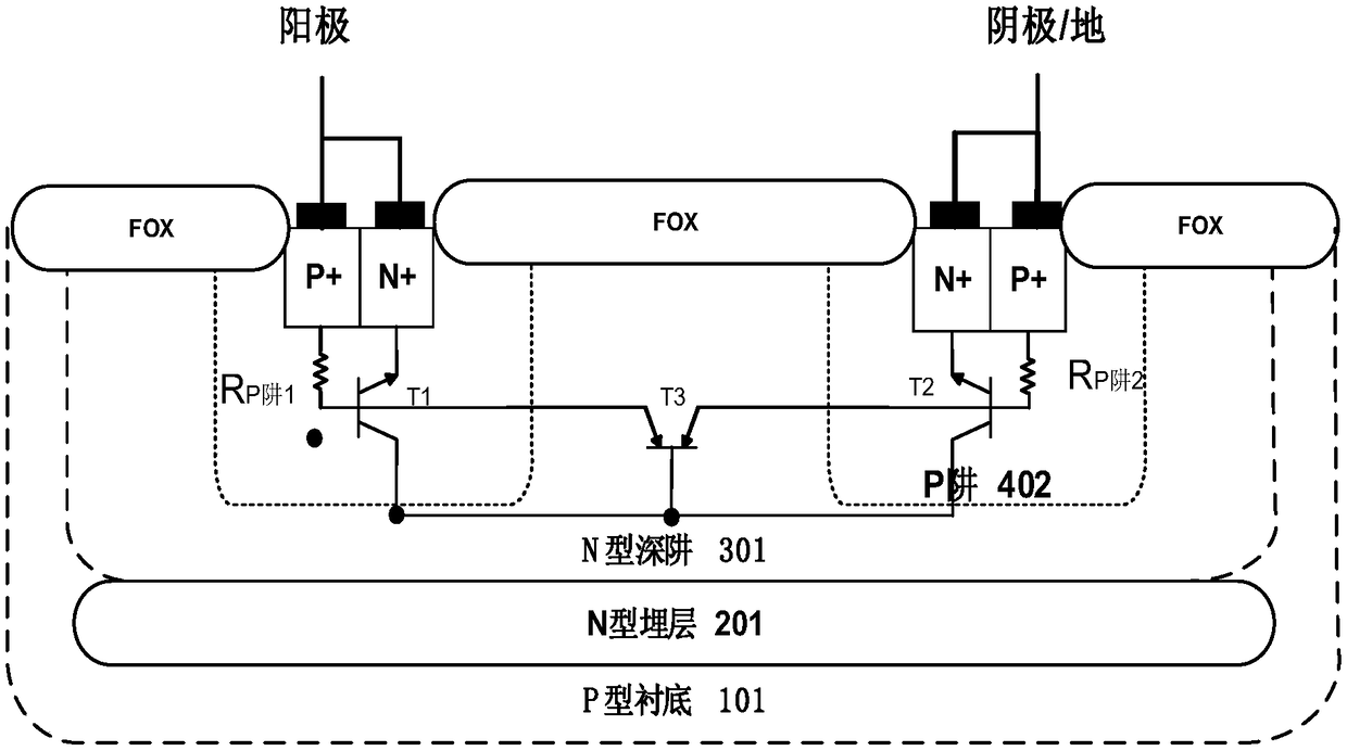
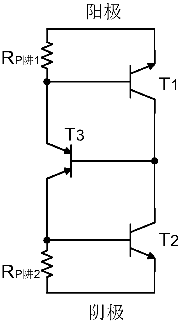
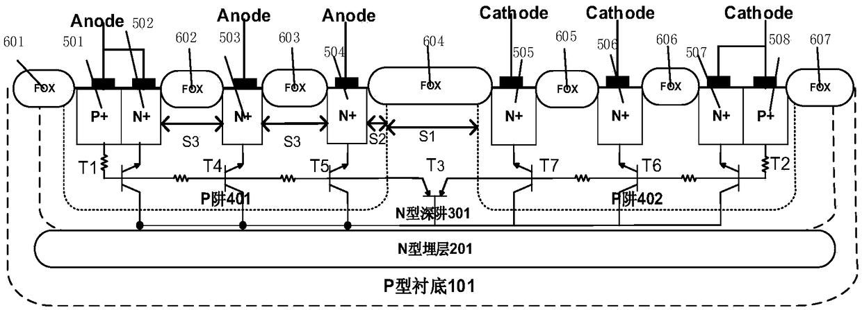
[0034] Such as image 3 As shown, a high-protection triac electrostatic protection device includes a P-type substrate 101; an N-type buried layer 201 is arranged in the substrate; an N-type deep well 301 is above the N-type buried layer 201 The left side of the N-type deep well 301 is provided with a first P well 401, and the right side of the N-type deep well 301 is provided with a second P well 402; the first P well 401 is sequentially provided with a first P+ injection region 501 and three N+ implantation regions I (respectively the first N+ implantation region 502, the second N+ implantation region 503, and the third N+ implantation region 504); the second P well 402 is sequentially provided with three N+ implantation regions II (respectively the fourth N+ implantation region 505, the fifth N+ implantation region 506, the sixth N+ implantation region...


PUM


Abstract

The invention discloses a bidirectional silicon-controlled electrostatic protection device with high protection level. The bidirectional silicon-controlled electrostatic protection device comprises aP-type substrate, wherein an N-type buried layer is arranged in the substrate, an N-type deep well is arranged on the N-type buried layer, a first P well and a second P well are arranged in the N-typedeep well, a first P+ injection region and a plurality of N+ injection regions I are arranged in the first P well, a second P+ injection region and a plurality of N+ injection regions II are arrangedin the second P well, the first P+ injection region and all N+ injection regions I are connected and used as a positive electrode of the device, and the second P+ injection region and all N+ injection regions II are connected and used as a negative electrode of the device. The numbers of the N+ injection regions I and the N+ injection regions II can be increased or reduced according to differentprotection levels, the numbers of the N+ injection regions I and the N+ injection regions II are increased if the protection level is high, the uniform current distribution of the device is improved,and the robustness of the device is improved; and if the protection level is low, the numbers of the N+ injection regions I and the N+ injection regions II are reduced, and the layout area is reduced.

Description

technical field [0001] The invention relates to the field of electrostatic protection, in particular to a bidirectional thyristor electrostatic protection device with high protection level and a manufacturing method thereof. Background technique [0002] With the advancement of semiconductor manufacturing technology, the failure of integrated circuit chips and electronic products caused by ESD has become more and more serious. ESD protection for electronic products and integrated circuit chips has become one of the main problems faced by product engineers. [0003] The failure modes caused by ESD include hard failure, soft failure and latent failure. The causes of these failures can be divided into electrical failures and thermal failures. The thermal failure refers to that when the ESD pulse comes, a current of a few amperes to tens of amperes is generated locally on the chip. The duration is short but a large amount of heat will be generated to melt the local metal conne...

Claims


Application Information

Patent Timeline
Patent Type & Authority Applications(China)
IPC IPC(8): H01L27/02
CPCH01L27/0262H01L27/0296
Inventor 汪洋夹丹丹杨红姣芦俊
Owner XIANGTAN UNIV
Why Eureka
Try Eureka