Novel ESD protection structure and realizing method thereof

A technology of ESD protection and implementation method, which is applied in the direction of electrical components, diodes, electric solid-state devices, etc., can solve the problem of increasing the overall area of ​​silicon-controlled rectifiers, and achieve the effect of increasing the maintenance voltage

Active Publication Date: 2017-10-13
SHANGHAI HUALI MICROELECTRONICS CORP
View PDF6 Cites 7 Cited by
  • Summary
  • Abstract
  • Description
  • Claims
  • Application Information

AI Technical Summary

Problems solved by technology

[0011] However, the disadvantage of the above-mentioned method of connecting forward-conducting diodes with parallel resistors is that each additional level of forward-conducting

Method used


Image

  • Novel ESD protection structure and realizing method thereof
  • Novel ESD protection structure and realizing method thereof
  • Novel ESD protection structure and realizing method thereof

Examples


Example Embodiment

[0037] The embodiments of the present invention will be described below through specific examples and in conjunction with the accompanying drawings, and those skilled in the art can easily understand other advantages and effects of the present invention from the contents disclosed in this specification. The present invention can also be implemented or applied through other different specific examples, and various details in this specification can also be modified and changed based on different viewpoints and applications without departing from the spirit of the present invention.

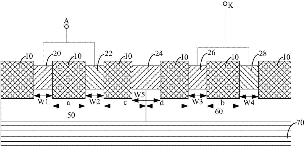
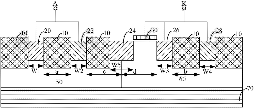
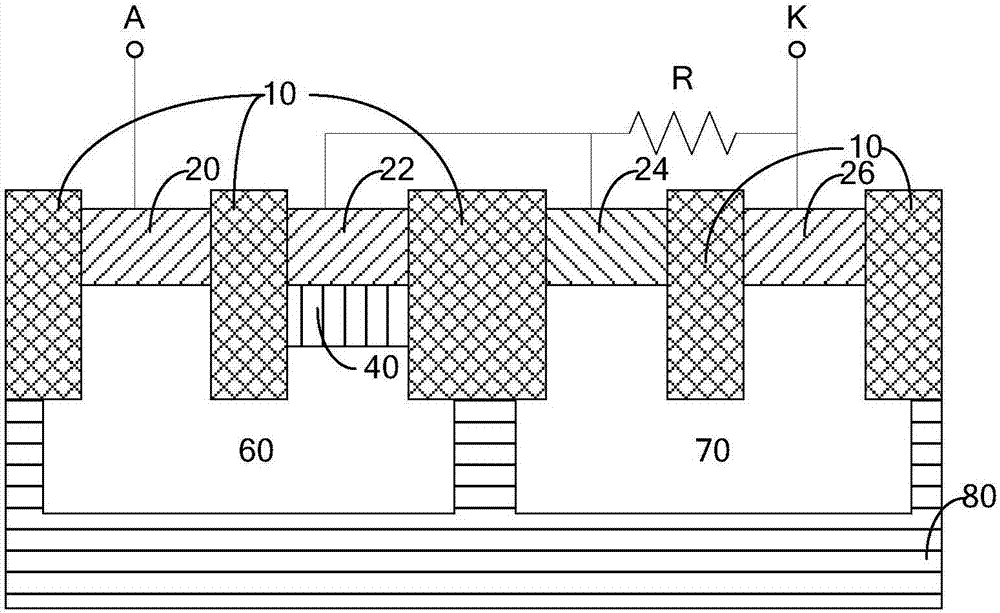
[0038] Figure 4 It is a circuit structure diagram of a preferred embodiment of a novel ESD protection structure of the present invention. like Figure 4 As shown, a novel ESD protection structure of the present invention includes an oxide layer (OX) 10, a high-concentration N-type doping (N+) 20, a high-concentration N-type doping (N+) 22, and a high-concentration P-type doping (P+ ) 24, high-con...


PUM

PropertyMeasurementUnit
Separation distanceaaaaaaaaaa

Abstract

The invention discloses a novel ESD (Electro-Static Discharge) protection structure and a realizing method thereof. The ESD protection structure comprises a semiconductor base body; a first N well and a second N well generated in the semiconductor base body; a silicon controlled rectifier arranged in the first N well and a diode structure arranged in the second N well; a high-concentration P-type doping (28), a high-concentration N-type doping (20) and a high-concentration N-type doping (22) arranged at the upper part of the first N well; and a P-type ESD implanting layer (40) arranged below the high-concentration N-type doping (22). The high-concentration N-type doping (20) is connected in a floating manner and has a distance S to the high-concentration P-type doping (28); the high-concentration N-type doping (20) and the high-concentration N-type doping (22) are arranged in an isolated manner; and the high-concentration P-type doping (28), the first N well (60), the ESD implanting layer (40) and the high-concentration N-type doping (22) compose the silicon controlled rectifier. According to the novel ESD protection structure and the realizing method thereof, the maintaining voltage of the hysteresis effect of the ESD protection structure can be increased.

Description

technical field [0001] The present invention relates to the technical field of semiconductor integrated circuits, in particular to a novel ESD protection structure with low trigger voltage and high sustain voltage and a method for realizing the same. Background technique [0002] In the field of electrostatic (ESD, Electro-Static Discharge) protection design, Silicon Controlled Rectifier (SCR, Silicon Controlled Rectifier) ​​is widely valued because of its strong ESD leakage capability and small parasitic capacitance. Serious defects limit its application: the first defect is that the trigger voltage of the hysteresis effect is very high, because its trigger voltage is mainly determined by the higher reverse breakdown voltage between the N-well and the P-well; the second defect is the return The hold voltage of the hysteresis effect is very low, which can easily lead to latch-up effect. [0003] In view of the defect of high trigger voltage, the industry has proposed variou...

Claims


Application Information

Patent Timeline
IPC IPC(8): H01L27/02
CPCH01L27/0248H01L27/0255
Inventor 朱天志
Owner SHANGHAI HUALI MICROELECTRONICS CORP
Why Eureka
Try Eureka