ESD protection component of LDMOS structure and with high maintaining voltage

A technology of ESD protection and high maintenance voltage, which is applied in the direction of electrical components, semiconductor devices, circuits, etc., can solve the problems of weak ESD robustness and insufficient anti-latch-up ability, so as to improve the secondary failure current, suppress the Kirk effect, The effect of improving high pressure resistance

Active Publication Date: 2014-04-09
扬州市冠科科技有限公司
View PDF3 Cites 9 Cited by
  • Summary
  • Abstract
  • Description
  • Claims
  • Application Information

AI Technical Summary

Problems solved by technology

[0004] Aiming at problems such as weak ESD robustness and insufficient latch-up resistance generally existing in existing high-voltage ESD protection devices, an example of the present invention designs an ESD protection device with a high sustain voltage LDOMS structure, which not only makes full use of the LDOMS The device can withstand the characteristics of high-voltage breakdown, and utilizes the layout level of the device through the specially designed P-sink doping, N-well, high-voltage N-well, P-well and N+ implantation, so that the device can form an SCR under the action of high-voltage ESD pulses. The structure of the ESD current discharge path, through the comprehensive trade-off and reasonable control of the layout parameters of the N+ / P sinking doped diode, can obtain high voltage resistance, high maintenance voltage, and strong robustness, which can be applied to ESD protection in high-voltage IC circuits device

Method used


Image

  • ESD protection component of LDMOS structure and with high maintaining voltage
  • ESD protection component of LDMOS structure and with high maintaining voltage
  • ESD protection component of LDMOS structure and with high maintaining voltage

Examples


Embodiment Construction

[0025] Below in conjunction with accompanying drawing and specific embodiment the present invention will be described in further detail:

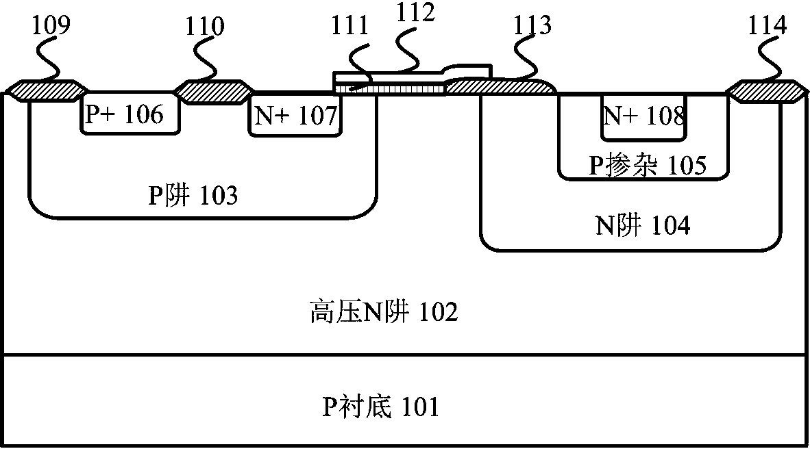
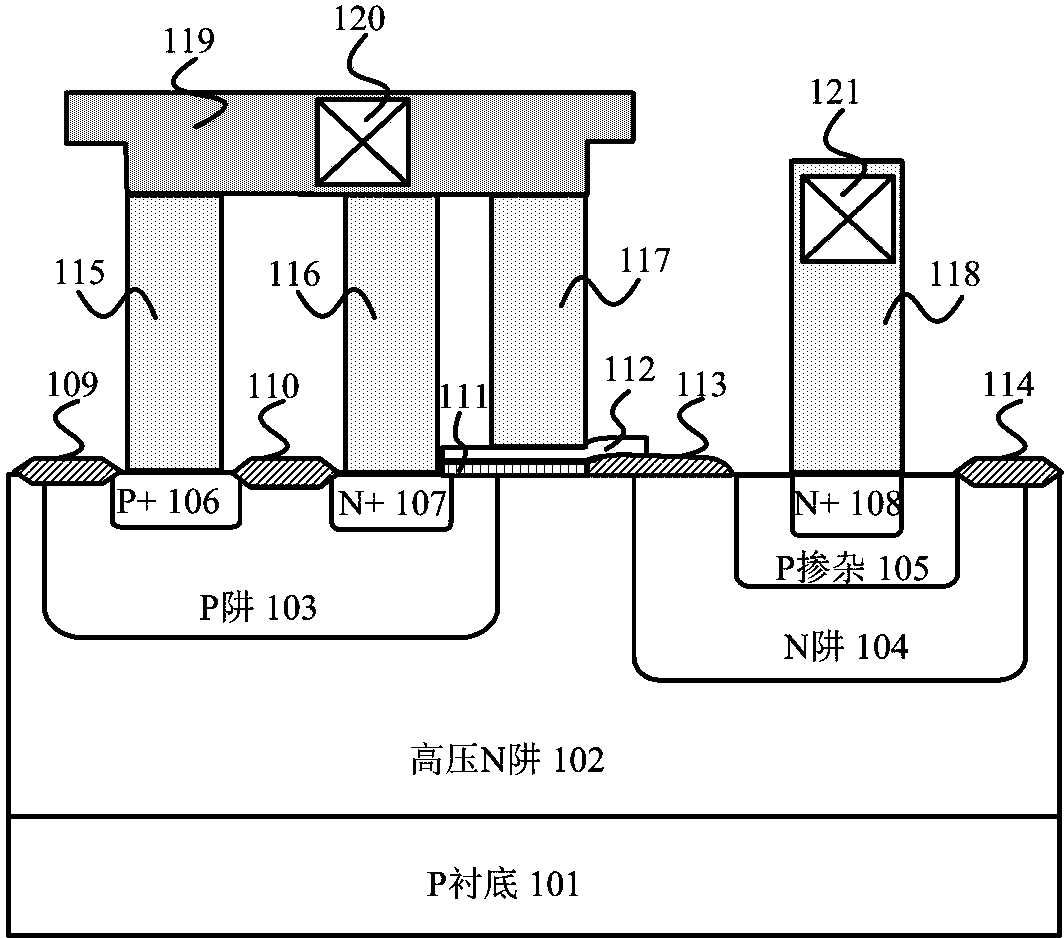
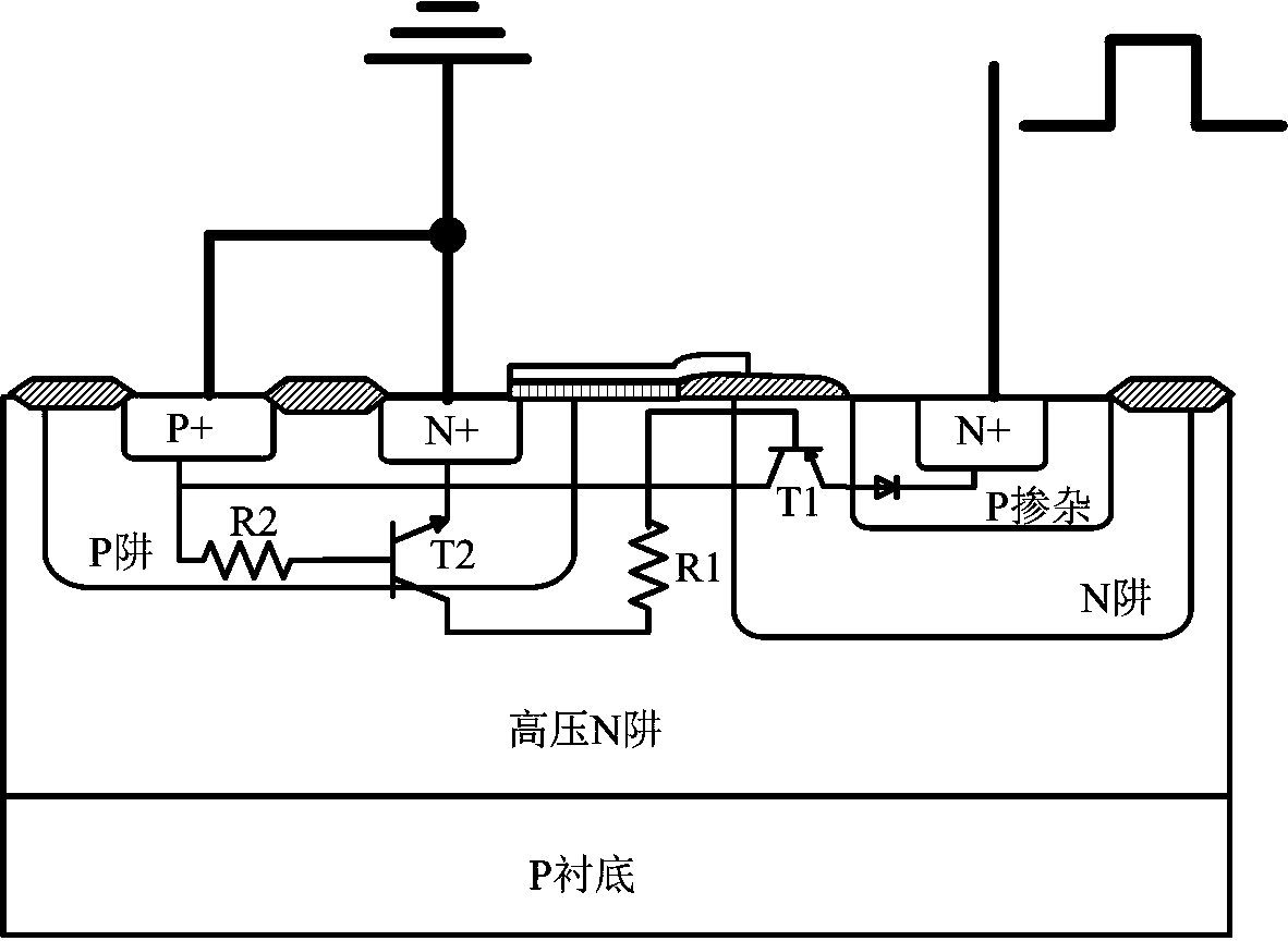
[0026] An example of the present invention designs an ESD protection device with an LDMOS structure of high sustaining voltage, which not only makes full use of the high-voltage resistance characteristics of the LDMOS device, but also utilizes the characteristics of the low on-resistance and large current discharge capability of the SCR device. Utilizing the special layout structure design of P sinking doping, and forming a PN junction structure with the second N+ implantation region, the maintenance voltage of the device can be increased, and the device can meet the needs of power integrated circuit products with different requirements by adjusting the key layout size. High voltage ESD protection, no latch-up effect.

[0027] Such as figure 1 The cross-sectional view of the internal structure of the device shown in the example of the pre...


PUM


Abstract

An ESD protection component of an LDMOS structure and with high maintaining voltage can be used for an on-chip IC high-voltage ESD protection circuit and mainly comprises a P substrate, a high-voltage N trap, an N trap, a P trap, a P sink doping, a P+ injection region, a first N+ injection region, a second N+ injection region, a meal anode, a metal cathode, a polysilicon gate, a thin gate oxide layer and a plurality of field oxide isolation regions. According to the ESD protection component of the LDMOS structure, under the action of an high-voltage ESD, on one hand, a parasitic SCR current discharging path is formed by the P sink doping, the N trap, the high-voltage N trap, the P trap and the first N+ injection region, idle currents of the component are increased, and ESD robustness of the component is improved; on the other hand, by means of a biasing reversal PN junction formed between the second N+ injection region and the P sink doping, maintaining voltage of the component is improved and the latch-up-resistant capacity of the component is improved.

Description

technical field [0001] The invention belongs to the field of electrostatic discharge protection of integrated circuits, relates to a high-voltage ESD protection device, in particular to an ESD protection device with a high sustain voltage LDMOS structure, which can be used to improve the reliability of on-chip IC high-voltage ESD protection. Background technique [0002] With the continuous development of power integration technology, power integrated circuit (IC) has become an important branch of the semiconductor industry. Lateral double diffused insulated gate field effect transistor (LDMOS) is a commonly used power device developed rapidly at the end of the last century. It is widely used in high-voltage and high-power circuit systems such as automotive electronics, power management, motor transmission, and various drive circuits. However, with the rapid development of semiconductor integration process, power integrated circuits suffer more and more serious damage from E...

Claims


Application Information

Patent Timeline
Patent Type & Authority Applications(China)
IPC IPC(8): H01L29/06H01L29/78
CPCH01L27/0266
Inventor 顾晓峰黄龙梁海莲毕秀文
Owner 扬州市冠科科技有限公司
Why Eureka
Try Eureka