Thyristor with high hold voltage and low triggering voltage ESD (electronstatic discharge) characteristic

A low trigger voltage, high sustain voltage technology, applied in thyristors, circuits, diodes, etc., can solve the problem that the sustain voltage does not meet the design requirements of ESD clamp protection devices, and achieve the effect of reducing the trigger voltage and increasing the sustain voltage.

Active Publication Date: 2011-11-16
SEMICONDUCTOR MANUFACTURING INTERNATIONAL (BEIJING) CORP +1
View PDF9 Cites 8 Cited by
  • Summary
  • Abstract
  • Description
  • Claims
  • Application Information

AI Technical Summary

Problems solved by technology

In this way, its maintenance voltage does not meet the design requirements of ESD clamp protection devices

Method used


Image

  • Thyristor with high hold voltage and low triggering voltage ESD (electronstatic discharge) characteristic
  • Thyristor with high hold voltage and low triggering voltage ESD (electronstatic discharge) characteristic
  • Thyristor with high hold voltage and low triggering voltage ESD (electronstatic discharge) characteristic

Examples


Embodiment 1

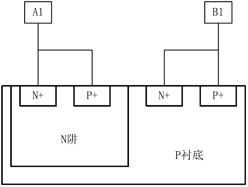
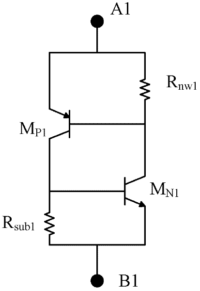
[0041] Figure 7 It is a specific structural schematic diagram of a thyristor with high sustain voltage and low trigger voltage ESD characteristics according to the first embodiment of the present invention. The thyristor includes from bottom to top: a substrate layer 311, a well region layer and a gate oxide layer. The well The region layer includes an N well region and a P well region, the N well region is adjacent to the P well region, and both the N well region and the P well region are in contact with the substrate layer 311, and the well region layer includes a N well region. Well region 309 and a P well region 310, the junction of the P well region 310 and the N well region 309 is provided with a first N+ doped region 305, and the N well region 309 is provided with a first P+ doped region 304, so The P well region 310 is provided with a second N+ doped region 306 and a second P+ doped region 307, the gate oxide layer is arranged on the upper surface of the well region l...

Embodiment 2

[0043] Figure 8 It is a specific structural diagram of a thyristor with high sustain voltage and low trigger voltage ESD characteristics according to the second embodiment of the present invention. On the basis of Embodiment 1, the preferred technical solution of the present invention is that the first P+ doping An insulating material region 313 is provided between the region 304 and the first N+ doped region 305 , and an insulating material region 313 is also provided between the second P+ doped region 307 and the second N+ doped region 306 .

Embodiment 3

[0045] Figure 9 It is a specific structural schematic diagram of a thyristor with high sustain voltage and low trigger voltage ESD characteristics according to the third embodiment of the present invention. The thyristor includes from bottom to top: a substrate layer 311, a well region layer and a gate oxide layer. The well The region layer includes an N well region and a P well region, the N well region is adjacent to the P well region, and both the N well region and the P well region are in contact with the substrate layer 311, and the well region layer includes a N well region. Well region 309 and two P well regions, the junction of the N well region 309 and the first P well region 310 is provided with a first N+ doped region 305, and the second P well region 308 is provided with a first P+ doped region 304, the first P well region 310 is provided with a second N+ doped region 306 and a second P+ doped region 307, the gate oxide layer is arranged on the upper surface of th...


PUM


Abstract

The invention relates to the technical field of a protection circuit of a semiconductor integrated chip, and particularly relates to a thyristor with high hold voltage and low triggering voltage ESD (electronstatic discharge) characteristic. The thyristor comprises a substrate layer (311), a well region layer and a gate oxide layer sequentially from bottom to top, wherein the well region layer comprises an N well region (309) and a P well region (310); the N well region is adjacent to the P well region; the N well region and the P well region contact the substrate layer (311); a first N+ doping region (305) is arranged at the junction of the N well region (309) and the P well region (310); the N well region (309) is provided with a first P+ doping region (304); and the P well region (310)is provided with a second N+ doping region (306) and a second P+ doping region (307). According to the invention, through improving the original thyristor structure, the triggering voltage of the thyristor is reduced, and the hold voltage of the thyristor is improved, so that the thyristor can ideally act as an ESD clamping protection device.

Description

technical field [0001] The invention relates to the technical field of protection circuits for semiconductor integrated chips, in particular to a thyristor with high sustain voltage and low trigger voltage ESD characteristics. Background technique [0002] In the manufacturing process of the integrated circuit IC chip and the final system application, there will be different degrees of electrostatic discharge (Electrostatic Discharge, ESD) events. Electrostatic discharge is an instantaneous process in which a large amount of charge is poured into the integrated circuit from the outside to the inside when an integrated circuit is floating. The whole process takes about 100ns to 200ns. In addition, when the integrated circuit is discharged, an equivalent high voltage of hundreds or even thousands of volts will be generated, which will break down the gate oxide layer of the input stage in the integrated circuit. As the size of MOS transistors in integrated circuits becomes sma...

Claims


Application Information

Patent Timeline
Patent Type & Authority Applications(China)
IPC IPC(8): H01L29/87H01L29/74H01L29/06
CPCH01L29/87
Inventor 张鹏王源贾嵩张钢刚张兴
Owner SEMICONDUCTOR MANUFACTURING INTERNATIONAL (BEIJING) CORP
Why Eureka
Try Eureka