Laterally diffused metal oxide semiconductor (LDMOS) transistor, layout method and manufacture method

A layout method and transistor technology, applied in semiconductor/solid-state device manufacturing, semiconductor devices, electrical components, etc., can solve problems such as inability to turn on

Active Publication Date: 2012-07-11
SEMICONDUCTOR MANUFACTURING INTERNATIONAL (BEIJING) CORP
View PDF8 Cites 8 Cited by
  • Summary
  • Abstract
  • Description
  • Claims
  • Application Information

AI Technical Summary

Problems solved by technology

[0008] In practice, it is found that when the above-mentioned LDMOS transistor is applied to ESD protection, the protected element often cannot be turned on under the normal operating voltage (operate voltage)

Method used


Image

  • Laterally diffused metal oxide semiconductor (LDMOS) transistor, layout method and manufacture method
  • Laterally diffused metal oxide semiconductor (LDMOS) transistor, layout method and manufacture method
  • Laterally diffused metal oxide semiconductor (LDMOS) transistor, layout method and manufacture method

Examples


Embodiment Construction

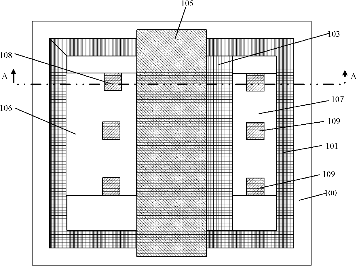
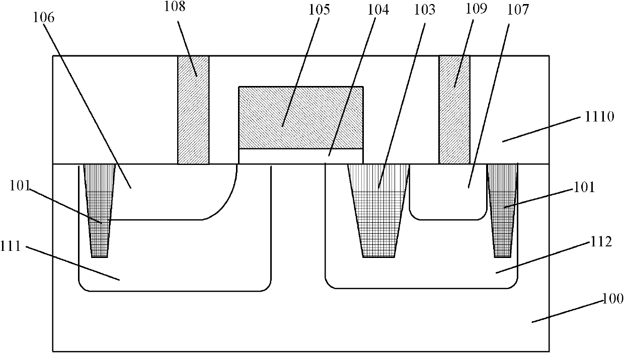
[0050] When the existing LDMOS transistor is applied to ESD protection, the drain region is connected to the IO pad of the element to be protected, and the drain region receives the input voltage signal of the IO pad. Such as figure 2 As shown, when the input voltage signal received by the drain region 107 is less than the maintenance voltage of the LDMOS transistor, the LDMOS transistor is in an off state; when the input voltage signal received by the drain region 107 is greater than or equal to the maintenance voltage of the LDMOS transistor, that is Electrostatic discharge occurs, so that the LDMOS transistor is turned on, thereby forming a conductive channel in the semiconductor substrate 100 below the gate 105, and the electrostatic discharge current passes through the second doped well 112, the conductive channel, and the first doped well 112 from the drain region 107. The heterowell 111 reaches the source region 106 and is grounded through the conductive plug 108 in th...


PUM


Abstract

The invention provides a structure of a laterally diffused metal oxide semiconductor (LDMOS) transistor, a manufacture method and a layout method of the structure. The structure comprises a substrate, a first mixing pit, a second mixing pit, a grid electrode structure, a first isolation structure, a second isolation structure, a source region, a drain region, an interlamination medium layer, a source region plug and a drain region plug. The first mixing pit and the second mixing pit are located in the substrate, the grid electrode structure is located above the first mixing pit and the second mixing pit, the isolation structure surrounds the first mixing pit and the second mixing pit, one side of the second isolation structure is adjacent to the grid electrode structure, the second isolation structure has two opposite ends and is connected with the first isolation structure, the source region is located in the first mixing pit, a third isolation structure is formed in the source region, and the source region is used for increasing resistance of the source region, the drain region is located in the second mixing pit between the first isolation structure and the second isolation structure, and the interlamination medium layer is located on the surface of the substrate, and the source region plug and the drain region plug are located in the interlamination medium layer. The structure guarantees that the LDMOS transistor can be normally opened.

Description

technical field [0001] The invention relates to the technical field of semiconductors, in particular to an LDMOS transistor, a layout method thereof, and a manufacturing method of the LDMOS transistor. Background technique [0002] In the development of power integrated circuits, the single-chip process developed to integrate power switches and control circuits, especially the lateral double diffusion MOS (lateral double diffusion MOS, LDMOS) process is a mainstream trend. The LDMOS process is planar diffusion on the surface of the semiconductor substrate to form the main lateral current path. Since LDMOS is manufactured in a typical IC process, the control circuit and LDMOS can be integrated on a monolithic power IC. LDMOS The process uses reduced surface electric field (RESURE) technology and low-thickness epitaxy (EPI) or N-type well region (N-well), which can achieve high voltage and low on-resistance. [0003] The LDMOS device is a field-effect transistor device (FET)...

Claims


Application Information

Patent Timeline
Patent Type & Authority Applications(China)
IPC IPC(8): H01L29/78H01L29/41H01L21/336H01L21/762H01L21/8234
CPCH01L29/7835H01L29/0653H01L29/0692
Inventor 曹国豪陈德艳郑大燮
Owner SEMICONDUCTOR MANUFACTURING INTERNATIONAL (BEIJING) CORP
Why Eureka
Try Eureka