
Elastic wave device and elastic wave module

a technology of elastic wave and elastic wave, which is applied in the direction of printed circuits, electrical apparatus, printed circuit non-printed electric components association, etc., can solve the problem of difficulty in achieving a sufficiently large out-of-band attenuation in the elastic wave device, and achieve the reduction of ground impedance of the first elastic wave filter, the isolation characteristics of the quadplexer including the first duplexer and the second duplexer can be significantly increased, and the attenuation is grea

Active Publication Date: 2017-08-03
MURATA MFG CO LTD
View PDF7 Cites 2 Cited by
  • Summary
  • Abstract
  • Description
  • Claims
  • Application Information

AI Technical Summary

Benefits of technology

The present invention relates to an elastic wave device with improved out-of-band attenuation. The technical effect achieved by the invention is to reduce the ground impedance of the first elastic wave filter and increase its out-of-band attenuation in a specific frequency band. This allows for a reduction in the size of the duplexer and improves isolation characteristics. Additionally, the elastic wave device includes first and second connection wirings that are designed to reduce the ground impedance of the first elastic wave filter. These technical effects improve the performance and reliability of the elastic wave device.

Problems solved by technology

Accordingly, it is difficult to achieve a sufficiently large out-of-band attenuation in the elastic wave device.

Method used


Image

  • Elastic wave device and elastic wave module
  • Elastic wave device and elastic wave module
  • Elastic wave device and elastic wave module

Examples


first preferred embodiment

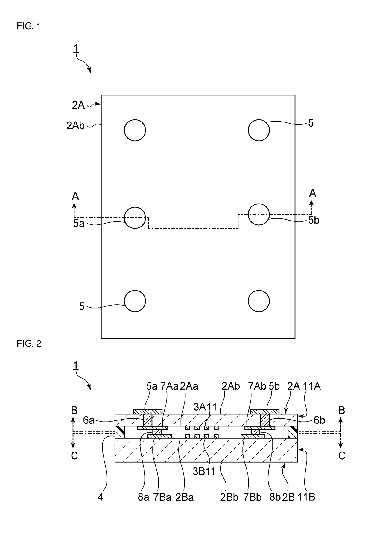
[0033]FIG. 1 is a plan view of an elastic wave device according to a first preferred embodiment of the present invention. FIG. 2 is a stair cross-sectional view at line A-A of FIG. 1.

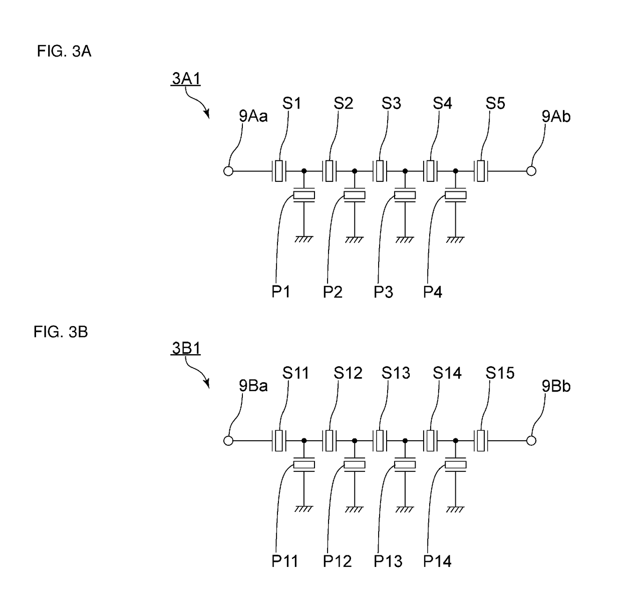
[0034]As depicted in FIG. 2, an elastic wave device 1 includes a first elastic wave element 11A and a second elastic wave element 11B. The first elastic wave element 11A includes a first piezoelectric substrate 2A. The first piezoelectric substrate 2A includes a first principal surface 2Aa and a second principal surface 2Ab disposed opposite to the first principal surface 2Aa. The second elastic wave element 11B includes a second piezoelectric substrate 2B. The second piezoelectric substrate 2B includes a first principal surface 2Ba and a second principal surface 2Bb. The thickness of the first piezoelectric substrate 2A is less than the thickness of the second piezoelectric substrate 2B. The first piezoelectric substrate 2A and the second piezoelectric substrate 2B include a piezoelectric single crysta...

second preferred embodiment

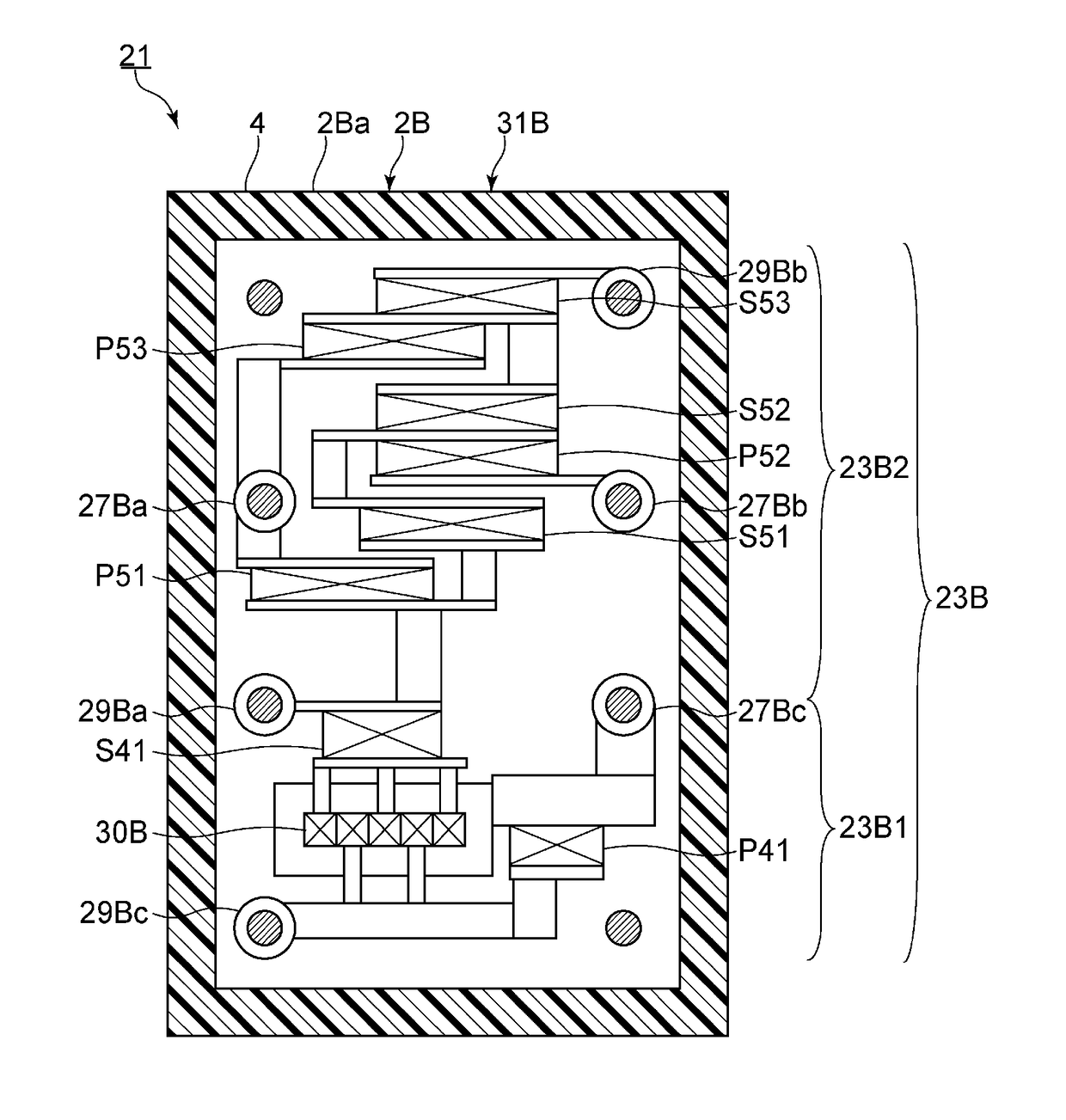
[0058]FIG. 8 is a top cross-sectional view depicting an electrode arrangement on a first principal surface of a first piezoelectric substrate according to a second preferred embodiment of the present invention. FIG. 9 is a top cross-sectional view depicting an electrode arrangement on a first principal surface of a second piezoelectric substrate in the second preferred embodiment.

[0059]An elastic wave device 21 of the second preferred embodiment includes a structure similar to the structure of the first preferred embodiment except the circuitry differs from the first preferred embodiment.

[0060]A first duplexer 23A is located on a first principal surface 2Aa of a first piezoelectric substrate 2A in a first elastic wave element 31A of the elastic wave device 21. The first duplexer 23A includes a first bandpass filter 23A1 that defines and functions as the first elastic wave filter and a second bandpass filter 23A2 whose passband is different from the passband of the first bandpass fil...

third preferred embodiment

[0074]FIGS. 13A-13D are circuit diagrams of a first bandpass filter to a fourth bandpass filter according to a third preferred embodiment of the present invention.

[0075]In the present preferred embodiment, the third bandpass filter 23B1 of the second preferred embodiment depicted in FIG. 10 is implemented as a third bandpass filter 43B1. Furthermore, the present preferred embodiment differs from the second preferred embodiment in the arrangement of the first to fourth bandpass filters 23A1, 23A2, 43B1, and 23B2. Except the foregoing features, elements, and components, the present preferred embodiment includes features, elements, and components similar to the features, elements, and components of the second preferred embodiment.

[0076]Specifically, the first bandpass filter 23A1 and the second bandpass filter 23A2 are located on a first principal surface of a second piezoelectric substrate. The third bandpass filter 43B1 and the fourth bandpass filter 23B2 are located on a first princ...


PUM


Abstract

An elastic wave device includes a first piezoelectric substrate including a first principal surface and a second principal surface, a second piezoelectric substrate including a first principal surface and a second principal surface and with a greater thickness than that of the first piezoelectric substrate, and ground terminals located on the second principal surface of the first piezoelectric substrate. The first principal surface of the first piezoelectric substrate and the first principal surface of the second piezoelectric substrate are joined to face each other. On the first principal surface of the first piezoelectric substrate, a first elastic wave filter is located. On the first principal surface of the second piezoelectric substrate, a second elastic wave filter is located. The out-of-band attenuation of the first elastic wave filter is greater than the out-of-band attenuation of the second elastic wave filter.

Description

CROSS REFERENCE TO RELATED APPLICATIONS[0001]This application claims the benefit of priority to Japanese Patent Application No. 2014-222762 filed on Oct. 31, 2014 and is a Continuation Application of PCT Application No. PCT / JP2015 / 078582 filed on Oct. 8, 2015. The entire contents of each application are hereby incorporated herein by reference.BACKGROUND OF THE INVENTION1. Field of the Invention[0002]The present invention relates to elastic wave devices, for example, bandpass filters and the like, and the present invention also relates to elastic wave modules.2. Description of the Related Art[0003]Elastic wave devices have been used as bandpass filters of cellular phones and the like.[0004]Japanese Unexamined Patent Application Publication No. 2008-546207 describes one example of such elastic wave devices. The elastic wave device of the Japanese Unexamined Patent Application Publication No. 2008-546207 includes two elastic wave elements. In each elastic wave element, an interdigital ...

Claims


Application Information

Patent Timeline
Patent Type & Authority Applications(United States)
IPC IPC(8): H03H9/64H03H9/145H05K1/18H03H9/25
CPCH03H9/6406H03H9/25H05K2201/1006H05K1/181H03H9/14541H03H9/0547H03H9/0576H03H9/6433H03H9/725
Inventor NAKAMURA, SOICHI
Owner MURATA MFG CO LTD
Learn More