Solar photovoltaic output optimizer circuit
- Summary
- Abstract
- Description
- Claims
- Application Information
AI Technical Summary
Benefits of technology
Problems solved by technology
Method used
Image
Examples
embodiment 1
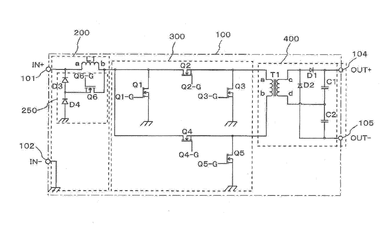
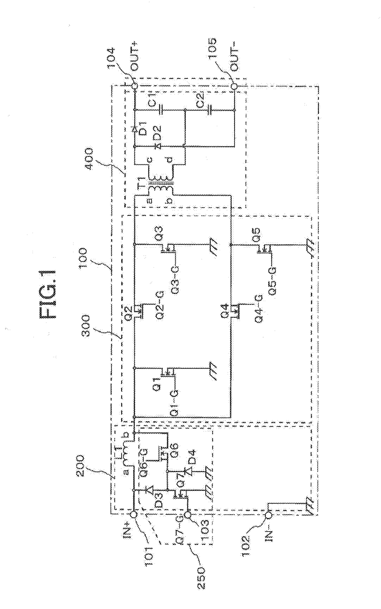
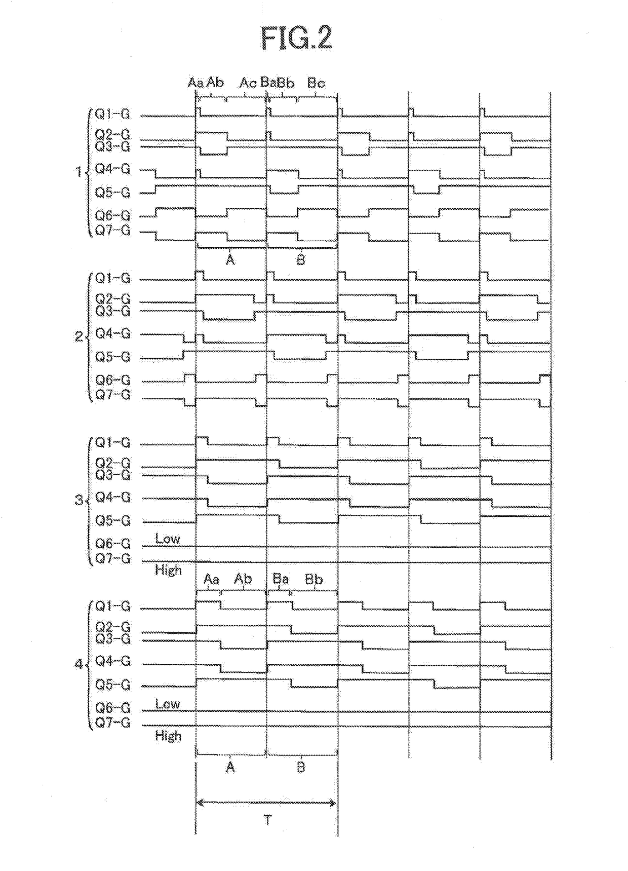
[0046]FIG. 1 is a circuit diagram for illustrating a configuration of Embodiment 1 of the PV optimizer of the present invention. FIG. 2 is an operation timing waveform diagram showing the levels of gate signals of switching transistors constituting the circuit in FIG. 1. FIG. 2 also includes the operation timing waveform described in the conventional art, in order to clarify the description of the operation of this embodiment. “4” in FIG. 2 corresponds to encircled 4 in FIG. 7, and “1” corresponds to encircled 1 in FIG. 8.
[0047]The PV optimizer circuit 100 according to Embodiment 1 of the present invention shown in FIG. 1 includes PV input means 200, switching means 300, and voltage doubler rectification means 400. The configurations of the switching means 300 and the voltage doubler rectification means 400 are analogous to those of the conventional PV optimizer described above. Some of the action and operation of the circuit depend on the description of the conventional art, and th...
embodiment 2
[0068]FIG. 3 is a circuit diagram for illustrating the configuration of Embodiment 2 of the solar photovoltaic output optimizer circuit of the present invention. In the aforementioned Embodiment 1, the input means 200 is provided with the surge protection circuit that includes the sixth switching transistor Q6 and the seventh switching transistor Q7. In Embodiment 2, the surge protection circuit provided for the input means 200 is configured by removing the seventh switching transistor Q7 from the circuit shown in FIG. 1 and by including only the sixth switching transistor Q6, the third diode D3 and the fourth diode D4.
[0069]The operation of the solar photovoltaic output optimizer circuit of Embodiment 2 of the present invention shown in FIG. 3 is that obtained by removing the portion corresponding to the seventh switching transistor Q7 in the description of Embodiment 1. That is, the circuit is that obtained by removing the high-side driver.
[0070]Also according to Embodiment 2, a c...
PUM
 Abstract
Description
Claims
Application Information
 - R&D
- Intellectual Property
- Life Sciences
- Materials
- Tech Scout
- Unparalleled Data Quality
- Higher Quality Content
- 60% Fewer Hallucinations
Browse by: Latest US Patents, China's latest patents, Technical Efficacy Thesaurus, Application Domain, Technology Topic, Popular Technical Reports.
© 2025 PatSnap. All rights reserved.Legal|Privacy policy|Modern Slavery Act Transparency Statement|Sitemap|About US| Contact US: help@patsnap.com


