Imaging panel, method of producing imaging panel, and x-ray imaging device
a technology imaging panel, which is applied in the direction of radio frequency controlled devices, instruments, television systems, etc., can solve the problems of coupling capacitance formation, operation property variation or malfunction of x-ray imaging panel, signal noise generation at data lines, etc., to suppress operation property variation and malfunction, and inhibit coupling capacitance formation
- Summary
- Abstract
- Description
- Claims
- Application Information
AI Technical Summary
Benefits of technology
Problems solved by technology
Method used
Image

Examples
embodiment 1
(Configuration)
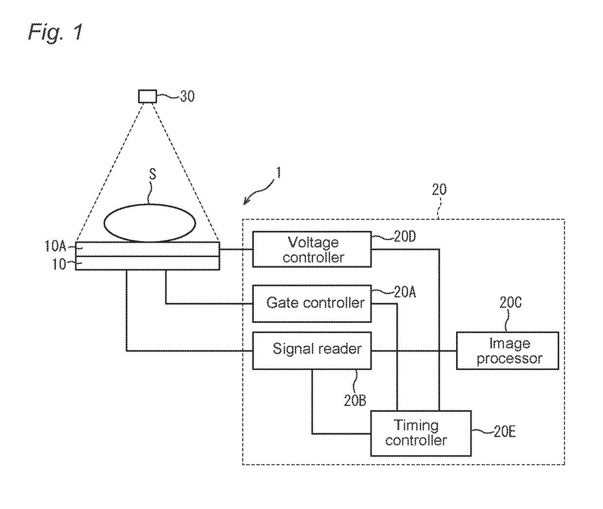
[0044]FIG. 1 is a pattern diagram of an X-ray imaging device 1 according to the embodiment 1. The X-ray imaging device 1 includes an imaging panel 10 and a controller 20. X-rays are applied from an X-ray source 30 to a target S, and the X-rays having been transmitted through the target S are converted to fluorescence (hereinafter, referred to as scintillation light) by a scintillator 10A disposed on the imaging panel 10. The X-ray imaging device 1 captures the scintillation light with use of the imaging panel 10 and the controller 20 to obtain an X-ray image.
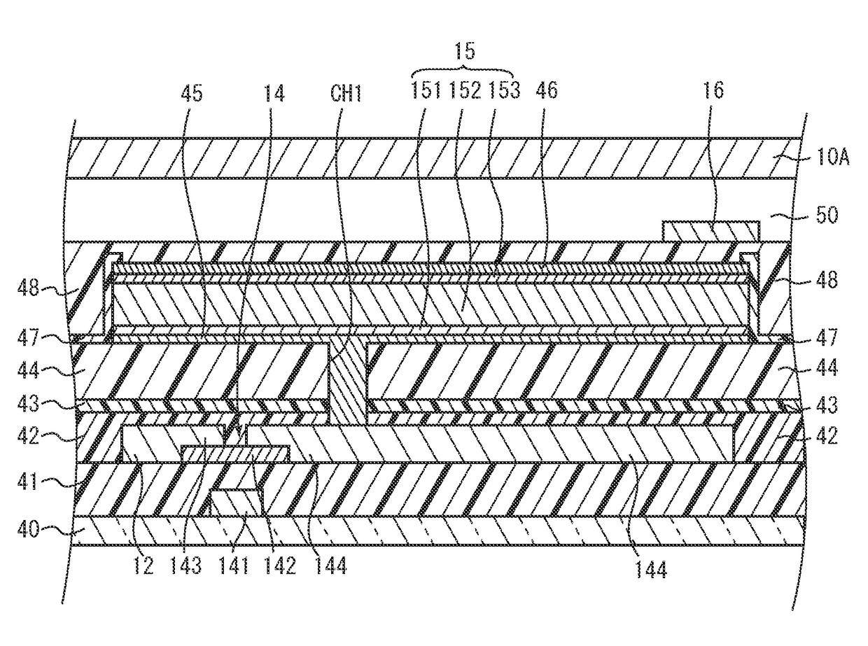
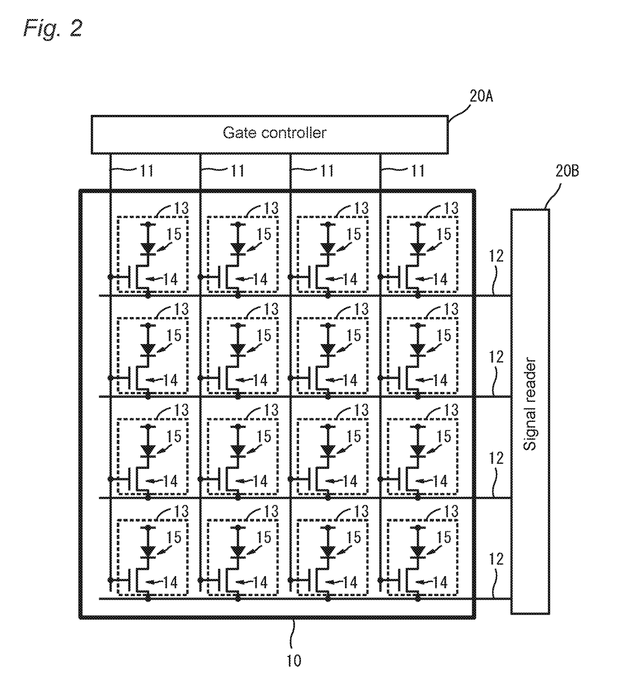
[0045]FIG. 2 is a pattern diagram depicting a schematic configuration of the imaging panel 10. As depicted in FIG. 2, the imaging panel 10 includes a plurality of gate lines 11 and a plurality of data lines 12 crossing the gate lines 11. The imaging panel 10 further includes a plurality of pixels 13 defined by the gate lines 11 and the data lines 12. FIG. 2 exemplifies the imaging panel 10 including 16 pixels 13 (...
embodiment 2
[0114]Described next is an X-ray imaging device according to the embodiment 2. The X-ray imaging device according to the embodiment 2 is configured identically to that according to the embodiment 1 except that part of the imaging panel 10 is configured differently.
[0115]The imaging panel 10 is configured identically to that according to the embodiment 1 except that the interlayer insulating film 44 is not the SOG film but a photosensitive resin film.
[0116]The photosensitive resin film provided as the interlayer insulating film 44 can be made of a photosensitive resist or a nonresist of a photosensitive resin. Examples of the photosensitive resist include a novolak resist and an ArF resist. Examples of the nonresist of a photosensitive resin include polyimide and polybenzimidazole.
[0117]The imaging panel 10 is produced in accordance with a method identical to the production method according to the embodiment 1 except for the process of producing the interlayer insulating film 44. In ...
modification examples
[0119]Modification examples of the present invention will be described below.
[0120]The above embodiments exemplify the imaging panel 10 including the TFTs 14 of the bottom gate type. Alternatively, the TFTs 14 can be of the top gate type as depicted in FIG. 17 or of the bottom gate type as depicted in FIG. 18.
[0121]A method of producing an imaging panel including the TFTs 14 of the top gate type of FIG. 17 will be described by referring to differences from the methods according to the above embodiments. Initially formed on the substrate 40 is the semiconductor active layer 142 made of an oxide semiconductor. The source electrode 143, the data line 12, and the drain electrode 144 are then formed by stacking titanium, aluminum, and titanium in the mentioned order on the substrate 40 and the semiconductor active layer 142.
[0122]The gate insulating film 41 made of a silicon oxide (SiOx), a silicon nitride (SiNx), or the like is subsequently formed on the semiconductor active layer 142, ...
PUM
 Abstract
Description
Claims
Application Information
 - R&D Engineer
- R&D Manager
- IP Professional
- Industry Leading Data Capabilities
- Powerful AI technology
- Patent DNA Extraction
Browse by: Latest US Patents, China's latest patents, Technical Efficacy Thesaurus, Application Domain, Technology Topic.
© 2024 PatSnap. All rights reserved.Legal|Privacy policy|Modern Slavery Act Transparency Statement|Sitemap