
Electromagnetic wave shielding tape using nanomaterials

Active Publication Date: 2017-08-17
ANDAQ TECH CO LTD
View PDF4 Cites 3 Cited by
  • Summary
  • Abstract
  • Description
  • Claims
  • Application Information

AI Technical Summary

Benefits of technology

The patent text describes an electromagnetic wave shielding tape that uses nanomaterials to provide protection against electromagnetic waves and static electricity. The tape includes a carrier substrate with two nanostructures on its surface, an insulating enclosing structure that protects the substrate and nanostructures, and an adhesive layer between the nanostructures. The tape can be used to shield electronic components from electromagnetic interference and to prevent static electricity build-up.

Problems solved by technology

In operation of an electronic device, a certain degree of electromagnetic field is generated, and electromagnetic fields generated by devices may interfere with each other or block each other, or normal operation of neighboring devices is affected.
Therefore, if the electromagnetic fields generated by a circuit current are not shielded appropriately, the electromagnetic fields may interfere with each other, and is the quality of signal transmission is deteriorated, so that the devices cannot be operated normally.

Method used


Image

  • Electromagnetic wave shielding tape using nanomaterials
  • Electromagnetic wave shielding tape using nanomaterials
  • Electromagnetic wave shielding tape using nanomaterials

Examples


first embodiment

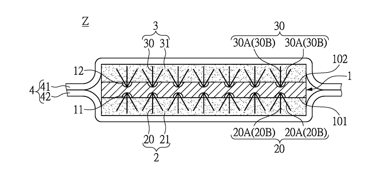
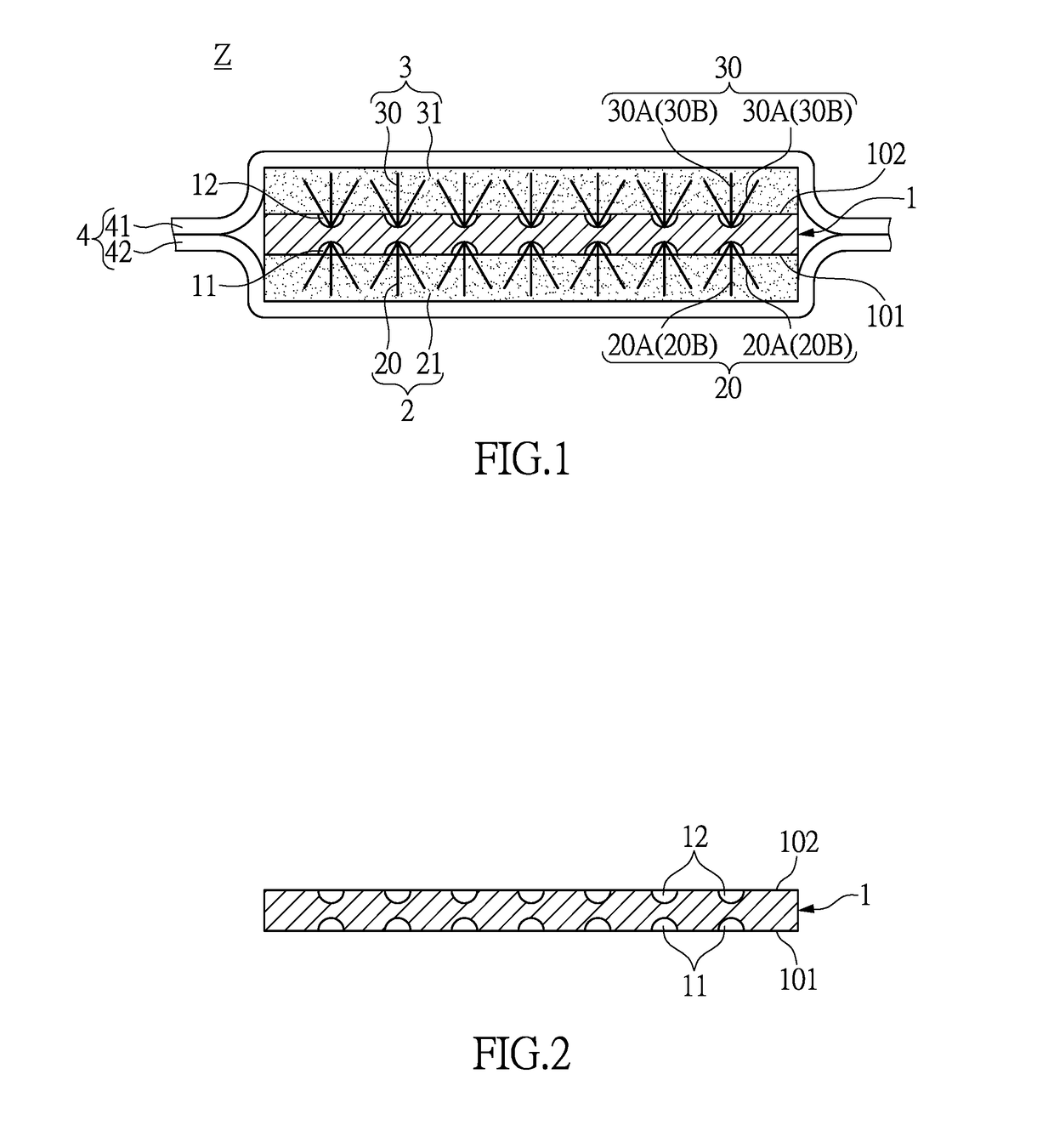
[0030]Referring to FIG. 1, FIG. 1 shows a lateral, cross-sectional, schematic view of the electromagnetic wave shielding tape using nanomaterials according to the first embodiment of the instant disclosure, the first embodiment of the instant disclosure provides an electromagnetic wave shielding tape Z using nanomaterials, comprising a carrier substrate 1, a first nanostructure 2, a second nanostructure 3 and an insulating enclosing structure 4. The carrier substrate 1 has a first surface 101 and a second surface 102 opposite to the first surface 101. The first nanostructure 2 is disposed on the first surface 101 of the carrier substrate 1, and the second nanostructure 3 is disposed on the second surface 102 of the carrier substrate 1. The insulating enclosing structure 4 includes a first insulating enclosing layer 41 and a second insulating enclosing layer 42 mated with each other, and the carrier substrate 1, the first nanostructure 2 and the second nanostructure 3 are enclosed by...

second embodiment

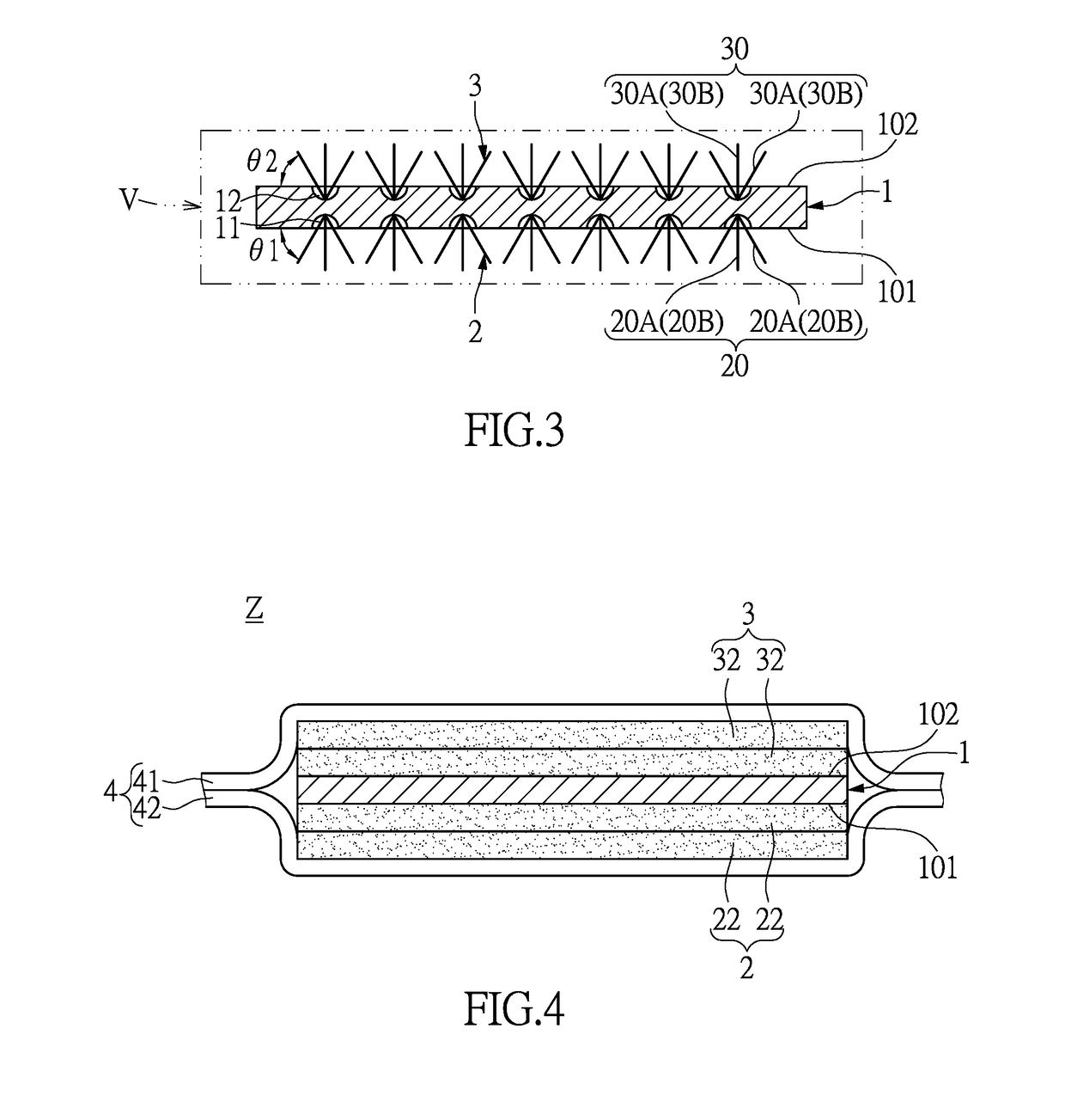
[0041]Referring to FIG. 4, FIG. 4 shows a lateral, cross-sectional, schematic view of the electromagnetic wave shielding tape using nanomaterials according to the second embodiment of the instant disclosure, and the second embodiment of the instant disclosure provides an electromagnetic wave shielding tape Z using nanomaterials, comprising a carrier substrate 1, a first nanostructure 2, a second nanostructure 3 and an insulating enclosing structure 4. Comparing FIG. 4 with FIG. 1, the difference between the second embodiment and the first embodiment is as follows: in the second embodiment, the first nanostructure 2 includes at least one first nanostructure coating layer 22 disposed on the first surface 101 of the carrier substrate 1 or a plurality of first nanostructure coating layers 22 stacked on top of one another and disposed on the first surface 101 of the carrier substrate 1, and the second nanostructure 3 includes at least one second nanostructure coating layer 32 disposed on...

third embodiment

[0043]Referring to FIG. 5, FIG. 5 shows a lateral, cross-sectional, schematic view of the electromagnetic wave shielding tape using nanomaterials according to the third embodiment of the instant disclosure, and the third embodiment of the instant disclosure provides an electromagnetic wave shielding tape Z using nanomaterials, comprising a carrier substrate 1, a first nanostructure 2, a second nanostructure 3 and an insulating enclosing structure 4. Comparing FIG. 5 with FIG. 1, the difference between the third embodiment and the first embodiment is as follows: in the third embodiment, the carrier substrate 1 may be a polymer network (or mesh) structure, the first nanostructure 2 includes at least one first nanostructure coating layer 22 disposed on the first surface 101 of the carrier substrate 1 or a plurality of first nanostructure coating layers 22 stacked on top of one another and disposed on the first surface 101 of the carrier substrate 1, and the second nanostructure 3 inclu...


PUM

PropertyMeasurementUnit
Timeaaaaaaaaaa
Mesh sizeaaaaaaaaaa

Abstract

An electromagnetic wave shielding tape using nanomaterials includes a carrier substrate, a first nanostructure, a second nanostructure, and an insulating enclosing structure for enclosing the carrier substrate, the first nanostructure, and the second nanostructure. The carrier substrate has a first surface and a second surface opposite to the first surface. The first nanostructure is disposed on the first surface of the carrier substrate, and the second nanostructure is disposed on the second surface of the carrier substrate.

Description

BACKGROUND OF THE INVENTION[0001]1. Field of the Invention[0002]The instant disclosure relates to an electromagnetic wave shielding tape, and more particularly to an electromagnetic wave shielding tape using nanomaterials.[0003]2. Description of Related Art[0004]In operation of an electronic device, a certain degree of electromagnetic field is generated, and electromagnetic fields generated by devices may interfere with each other or block each other, or normal operation of neighboring devices is affected. Therefore, if the electromagnetic fields generated by a circuit current are not shielded appropriately, the electromagnetic fields may interfere with each other, and is the quality of signal transmission is deteriorated, so that the devices cannot be operated normally.[0005]As a manner for electronic devices to resist electromagnetic interference, an electromagnetic interference (EMI) shielding material is used as a shielding cover for resisting the electromagnetic interference. T...

Claims


Application Information

Patent Timeline
IPC IPC(8): H05K9/00B32B3/30B32B7/04
CPCH05K9/0081B32B7/04B32B2457/04B32B2307/212B32B2307/206B32B3/30B32B5/028B32B5/22B32B5/26B32B7/12B32B9/007B32B9/04B32B15/04B32B27/08H05K9/0088B32B2250/02B32B2250/24B32B2250/44B32B2255/06B32B2255/10B32B2255/28B32B2262/103B32B2262/106B32B2307/538H05K9/009
Inventor LIN, CHING-FENG
Owner ANDAQ TECH CO LTD
Features
  • Generate Ideas
  • Intellectual Property
  • Life Sciences
  • Materials
  • Tech Scout
  • Unparalleled Data Quality
  • Higher Quality Content
  • 60% Fewer Hallucinations
Learn More