3-d stacked memory with reconfigurable compute logic

a compute logic and memory device technology, applied in the field of 3dstacked memory devices with reconfigurable compute logic, can solve the problems of high power consumption, general limitation of base dies, and low memory access latency

Active Publication Date: 2017-09-07
SAMSUNG ELECTRONICS CO LTD
View PDF5 Cites 35 Cited by
  • Summary
  • Abstract
  • Description
  • Claims
  • Application Information

AI Technical Summary

Benefits of technology

[0027]In an embodiment, the method may further include: receiving a mode register set command through a control bus of the interface from a host; and in response to receiving the mode register set command, configuring a PIM mode to compute the data.
[0028]In an embodiment, the method may further include: receiving a first memory command from the host through the control bus; translating the first memory command into the logic commands; and computing the data according to the logic commands.
[0029]In an embodiment, the method may further include: configuring a normal mode; receiving a second memory command from the host through the control bus; and performing a memory function according to the second memory command.
[0030]According to one or more exa

Problems solved by technology

The base die is generally limited to performing support logic for reading and writing data to the memory dies.
Generally, a processor and memory are separate, and thus, to transfer data therebetween results in memory access latency and high power consumption.
While general purpose processors provide flexibility, they are often more complex, costly, and

Method used


Image

  • 3-d stacked memory with reconfigurable compute logic
  • 3-d stacked memory with reconfigurable compute logic
  • 3-d stacked memory with reconfigurable compute logic

Examples


Embodiment Construction

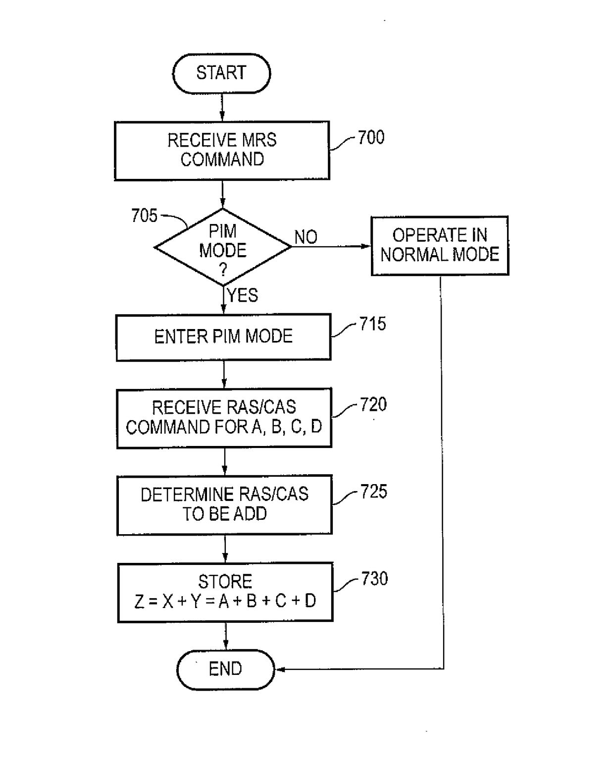
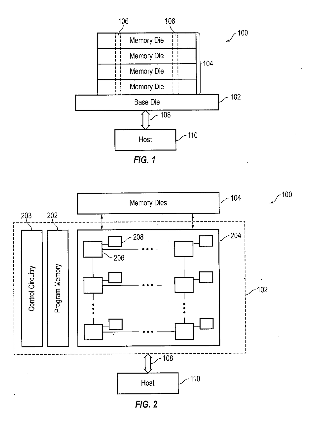
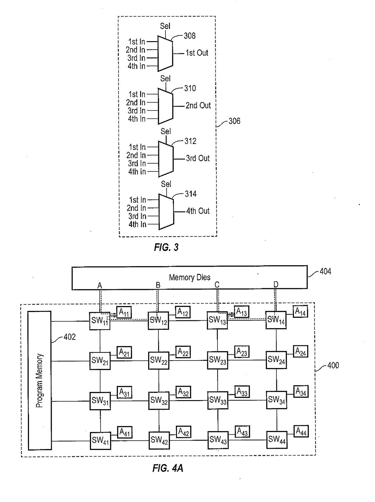
[0039]Hereinafter, example embodiments will be described in more detail with reference to the accompanying drawings, in which like reference numbers refer to like elements throughout. The present invention, however, may be embodied in various different forms, and should not be construed as being limited to only the illustrated embodiments herein. Rather, these embodiments are provided as examples so that this disclosure will be thorough and complete, and will fully convey the aspects and features of the present invention to those skilled in the art. Accordingly, processes, elements, and techniques that are not necessary to those having ordinary skill in the art for a complete understanding of the aspects and features of the present invention may not be described. Unless otherwise noted, like reference numerals denote like elements throughout the attached drawings and the written description, and thus, descriptions thereof may not be repeated.

[0040]In the drawings, the relative sizes...


PUM


Abstract

A 3D-stacked memory device including: a base die including a plurality of switches to direct data flow and a plurality of arithmetic logic units (ALUs) to compute data; a plurality of memory dies stacked on the base die; and an interface to transfer signals to control the base die.

Description

CROSS-REFERENCE TO RELATED APPLICATION[0001]This utility patent application claims priority to and the benefit of U.S. Provisional Patent Application Ser. No. 62 / 301,966, filed Mar. 1, 2016, entitled “3D-STACKED MEMORY WITH RECONFIGURABLE COMPUTE LOGIC,” the entire content of which is incorporated herein by reference.BACKGROUND[0002]1. Field[0003]One or more aspects of example embodiments of the present invention relate to a 3D-stacked memory device with reconfigurable compute logic.[0004]2. Description of the Related Art[0005]3D-stacked (3DS) memory is a high density and high performance memory structure that generally includes multiple layers of memory dies stacked on a base die that are interconnected using through silicon vias (TSVs). The base die is generally limited to performing support logic for reading and writing data to the memory dies. Examples of 3DS memory include hybrid memory cube (HMC) and high bandwidth memory (HBM).[0006]Generally, a processor and memory are separ...

Claims


Application Information

Patent Timeline
IPC IPC(8): G06F3/06G06F9/30
CPCG06F3/0605G06F3/0611G06F3/0625G06F9/30196G06F3/0659G06F3/0673G06F3/0635G06F15/785Y02D10/00G11C5/04G11C7/1006G06F13/14G06F13/40
Inventor CHANG, MU-TIENGERA, PRASUNNIU, DIMINZHENG, HONGZHONG
Owner SAMSUNG ELECTRONICS CO LTD
Why Eureka
Try Eureka