Baw device and baw device manufacturing method

a technology of baw device and manufacturing method, which is applied in the direction of impedence network, basic electric elements, electric apparatus, etc., can solve the problems of increasing environmental burden, and achieve the effect of less loss and higher power resistan

Inactive Publication Date: 2017-09-07
DISCO CORP
View PDF3 Cites 3 Cited by
  • Summary
  • Abstract
  • Description
  • Claims
  • Application Information

AI Technical Summary

Benefits of technology

[0006]In recent years, as an advanced form of SAW devices, BAW devices (BAW filters) utilizing a BAW propagated through the inside of a material have been drawing attention. A BAW device includes a resonator (piezoelectric element) wherein a piezoelectric film including a piezoelectric material such as aluminum nitride (AlN) is sandwiched between electrodes including molybdenum (Mo) or the like. The resonator is formed on a substrate including a semiconductor material such as silicon (Si). Unlike the SAW device, the BAW device does not have a comb-shaped electrode structure and, therefore, is advantageous from the viewpoint of lesser loss and higher power resistance. In addition, since the BAW device does not need to use a crystalline substrate including a piezoelectric material, it can be formed integrally with other active devices.

Problems solved by technology

However, when etching is adopted for removing the mechanical strains generated by the grinding, burden on environments is increased.

Method used


Image

  • Baw device and baw device manufacturing method
  • Baw device and baw device manufacturing method
  • Baw device and baw device manufacturing method

Examples


Embodiment Construction

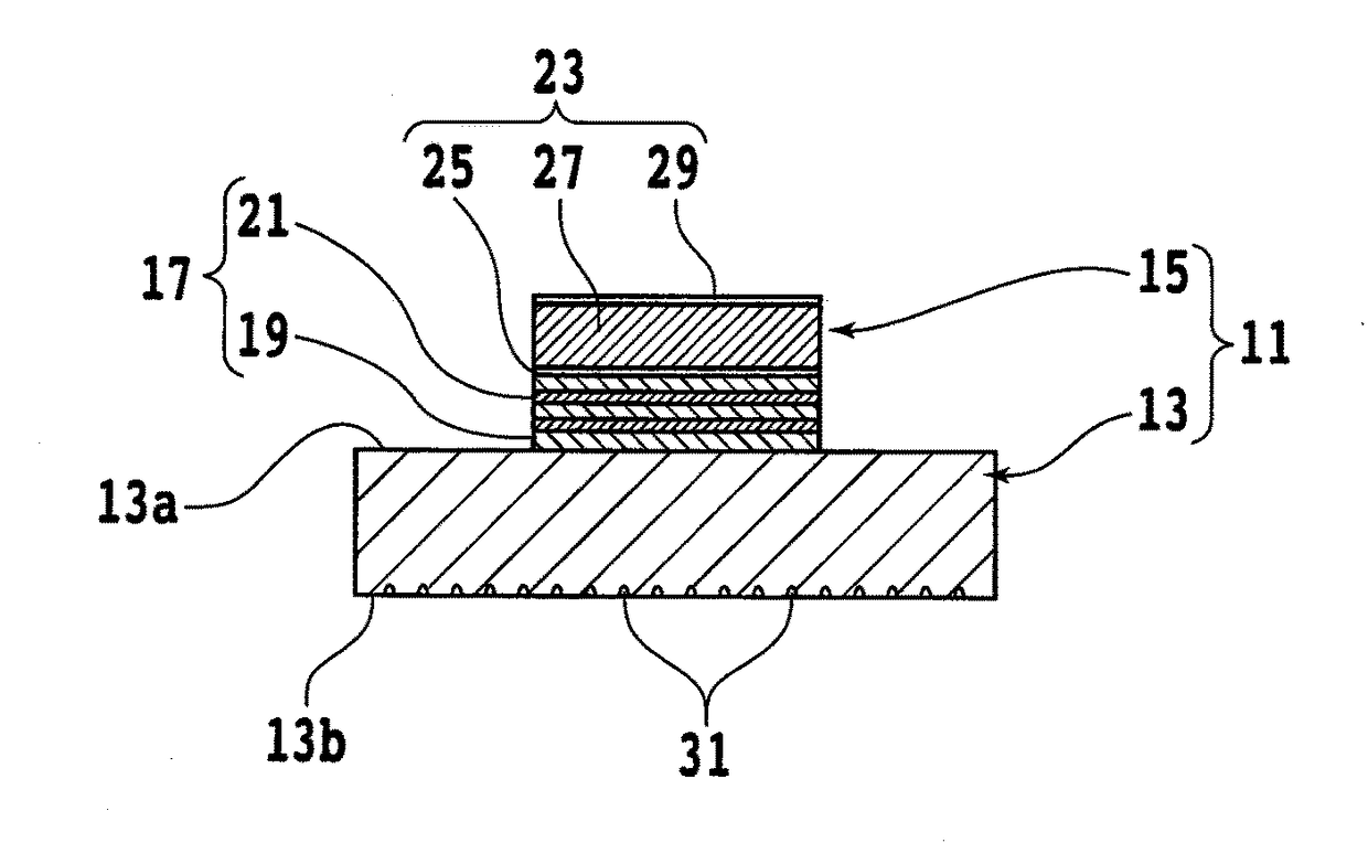
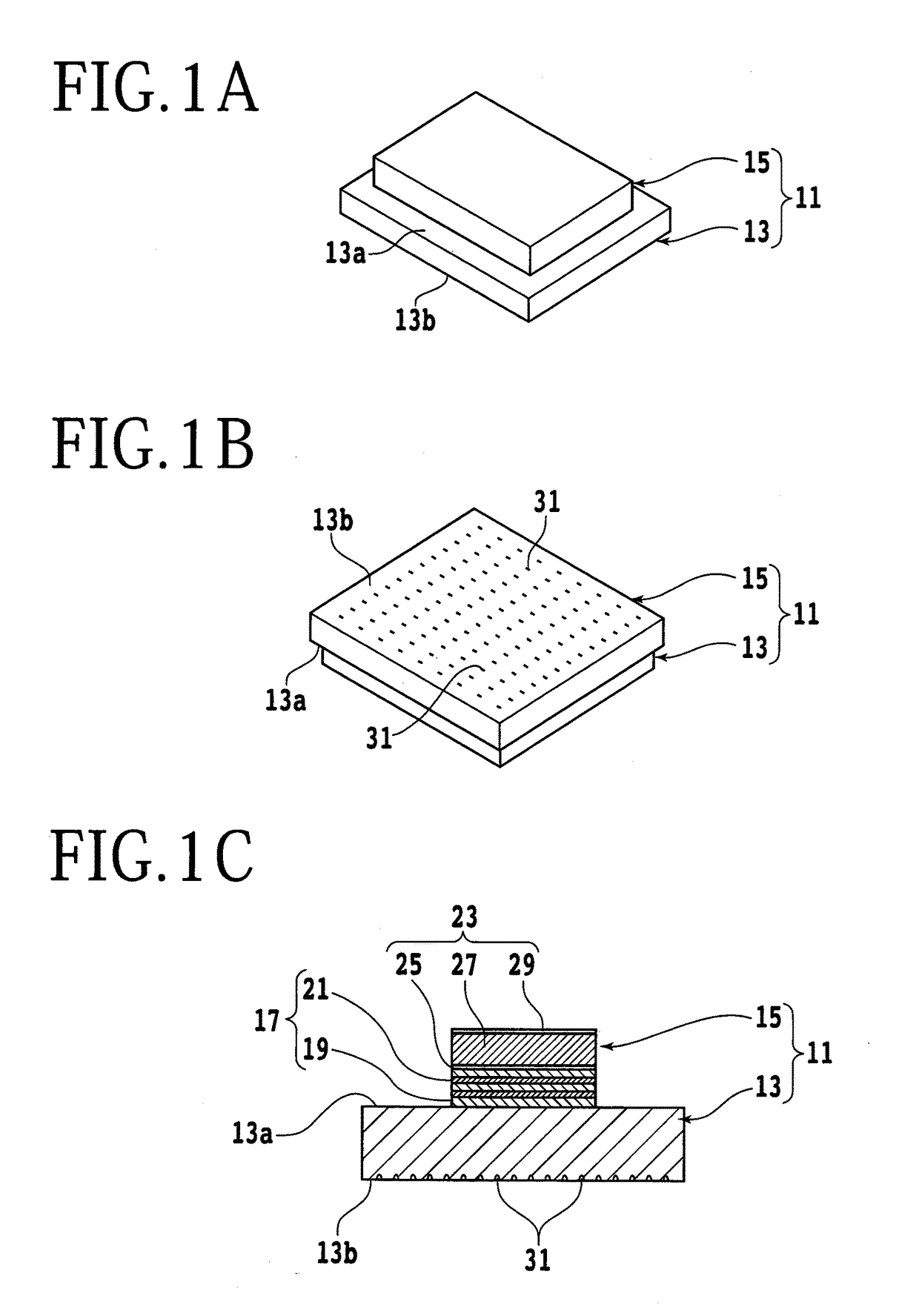
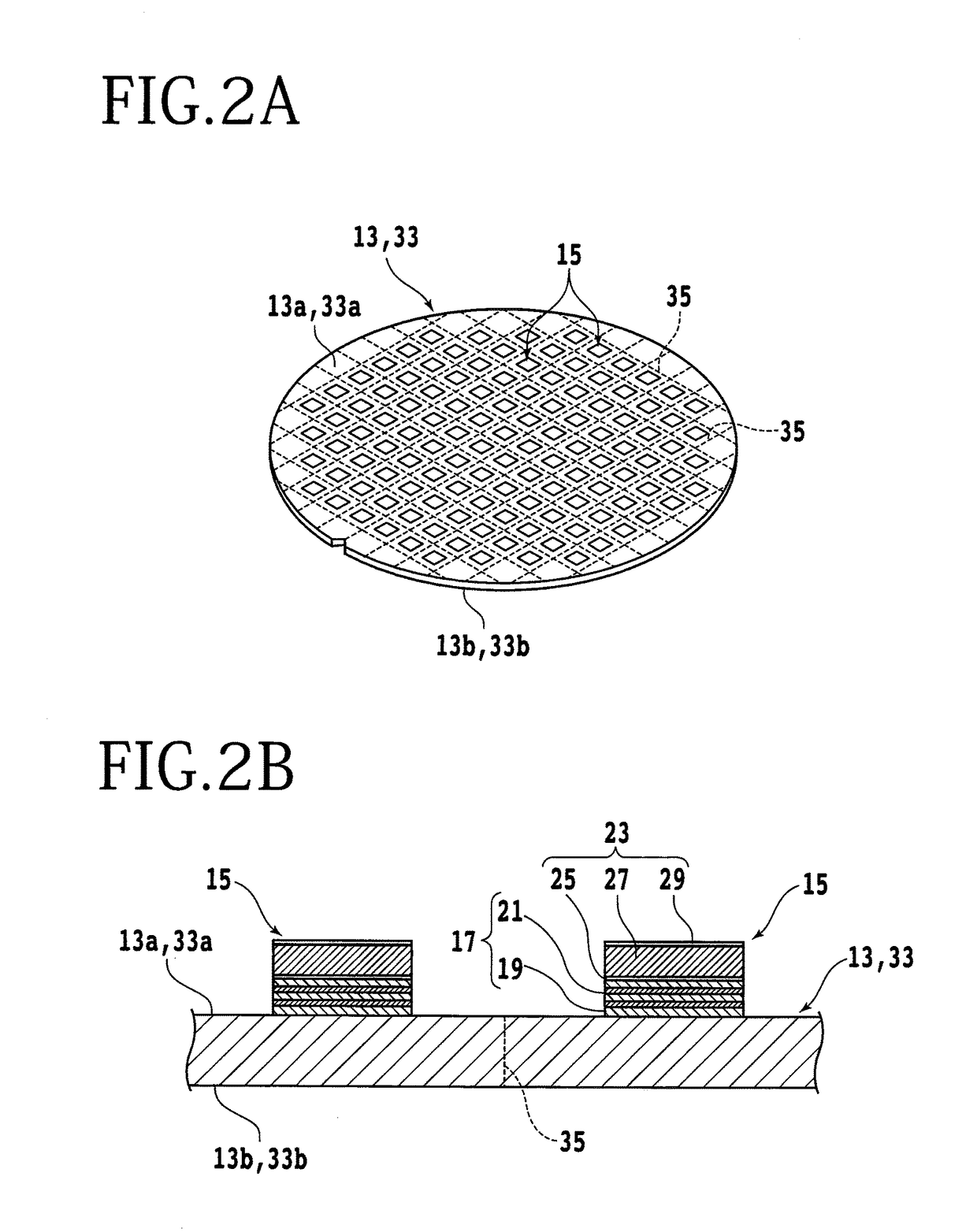
[0022]An embodiment of the present invention will be described below referring to the attached drawings. FIG. 1A is a perspective view showing schematically an upper-side external appearance of a BAW device; FIG. 1B is a perspective view showing schematically a lower-side external appearance of the BAW device; and FIG. 10 is a sectional view showing schematically a stack structure of the BAW device.

[0023]As illustrated in FIGS. 1A, 1B, and 1C, a BAW device (BAW device chip) 11 according to the present embodiment includes a rectangular substrate 13 including a semiconductor material such as crystalline silicon (Si). On a first surface (front surface) 13a of the substrate 13, there is provided a resonance unit 15 wherein films having various functions are stacked. The resonance unit 15 includes an acoustic multilayer film 17 formed on the lower side (the substrate 13 side). The acoustic multilayer film 17 is formed by stacking on each other a first film 19 including a material having ...


PUM


Abstract

A BAW device including a substrate, and a piezoelectric element formed on a front surface of the substrate is provided. The substrate is provided on a back surface side thereof with an acoustic wave diffusion region including a recess formed by partially melting a back surface of the substrate.

Description

BACKGROUND OF THE INVENTION[0001]Field of the Invention[0002]The present invention relates to a bulk acoustic wave (BAW) device utilizing a BAW propagated through the inside of a material, and a manufacturing method thereof.[0003]Description of the Related Art[0004]In telecommunication apparatuses such as a mobile phones, bandpass filters permitting electrical signals in a desired frequency band to pass therethrough play an important role. As one of the bandpass filters, there has been known a surface acoustic wave (SAW) device (SAW filter) utilizing a SAW. A SAW device includes a crystalline substrate including a piezoelectric material such as quartz (SiO2), and a comb-shaped electrode (inter digital transducer (IDT)) formed on a surface of the crystalline substrate, and permits passage therethrough of only electrical signals in a frequency band which is determined according to the kind of the piezoelectric material, the interval of the electrodes, etc.[0005]Meanwhile, in the SAW d...

Claims


Application Information

Patent Timeline
Patent Type & Authority Applications(United States)
IPC IPC(8): H03H9/17H03H9/54H03H3/02
CPCH03H9/17H03H9/54H03H3/02H10N30/10513H10N30/085H03H9/175H03H2003/025H03H9/172H03H9/0014H03H9/0095H01L21/263
Inventor ABATAKE, JUN
Owner DISCO CORP
Why Eureka
Try Eureka