Scanning Electron Microscope

Active Publication Date: 2017-10-26
HITACHI HIGH-TECH CORP
View PDF6 Cites 7 Cited by
  • Summary
  • Abstract
  • Description
  • Claims
  • Application Information

AI Technical Summary

Benefits of technology

This patent describes a way to get a high-quality image using a combination of a CFE electron source and a boosting process. This method ensures better current stability and higher resolution at lower power levels. The technical effect of this invention is to improve the image quality and stability of electron sources used in image formation processes.

Problems solved by technology

Currently, although an SE electron source is used in a commercial SEM with a boosting process, while current stability of the SE electron source is very high (2% / hr or less), energy width thereof is as wide as 0.6 eV, and resolution characteristics are significantly deteriorated at low accelerating voltage (in particular, at 1 kV or less).
Then, the inventors have pursued design and development to achieve the world's first commercial SEM with a combination of a CFE electron source and a boosting process; however, when the inventors combined a CFE electron source and a boosting process, they found that electric potential distribution around an extracting electrode and an anode electrode that form the electron source is more easily changed than a case in which a CFE electron source is not combined with a boosting process and that the amount of residual gas around the electron source becomes extremely large to lower current stability.
By the way, PTL 4 does not disclose a technical problem unique to a combination of a CFE electron source and a boosting process that the inventors have found (relationship between a cause or generation of residual gas and decrease in current stability).
Note that, because NEG pump has a disadvantage that it cannot exhaust chemically stable gas such as Ar and CH4, current stability is not improved only with a NEG pump.

Method used


Image

  • Scanning Electron Microscope
  • Scanning Electron Microscope
  • Scanning Electron Microscope

Examples


first example

(1) FIRST EXAMPLE

(1-1) Device Structure

[0040](Entire structure)

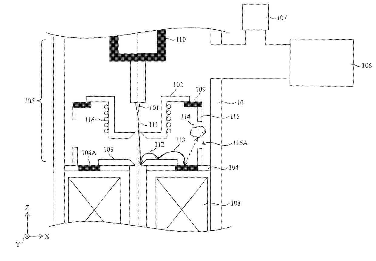
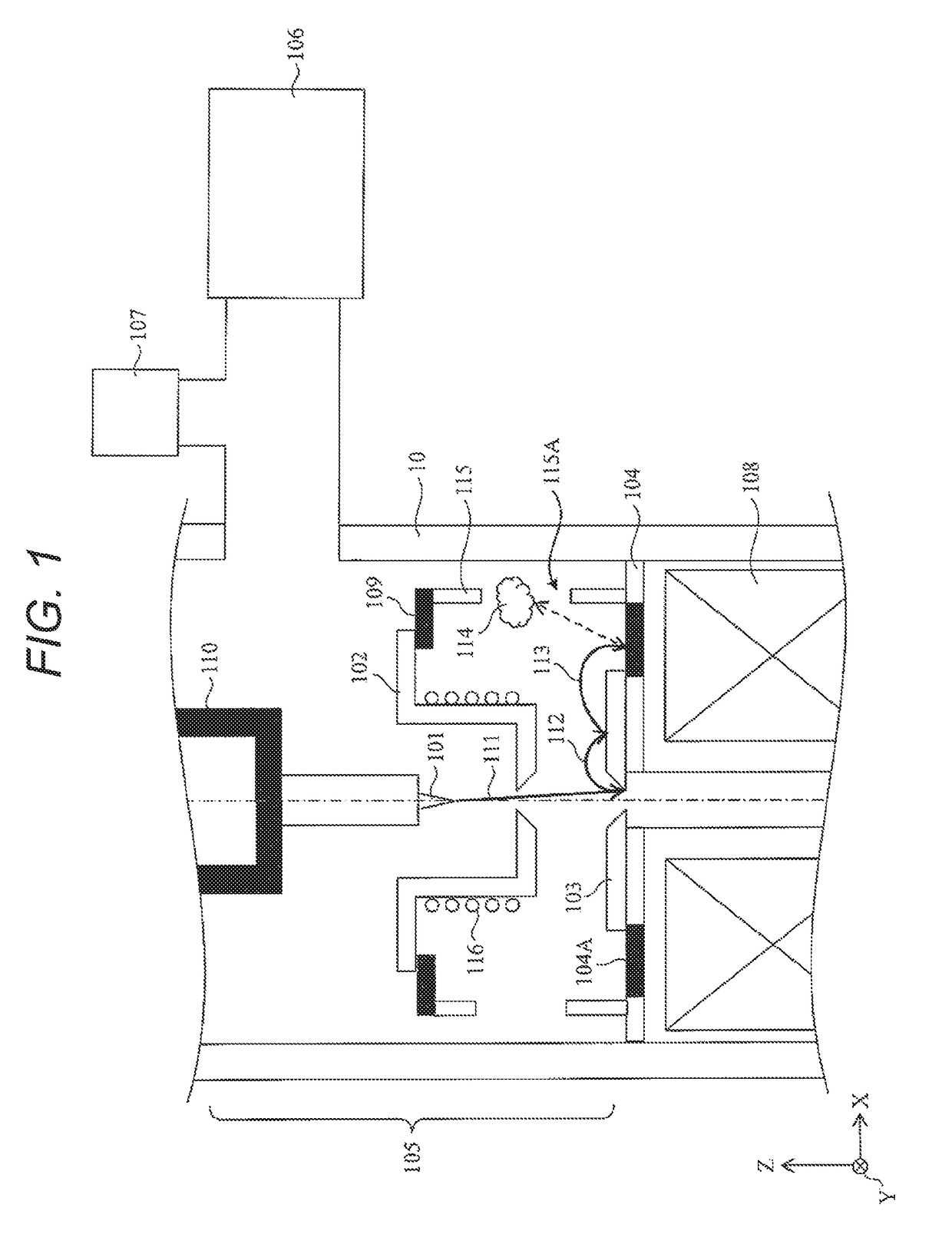
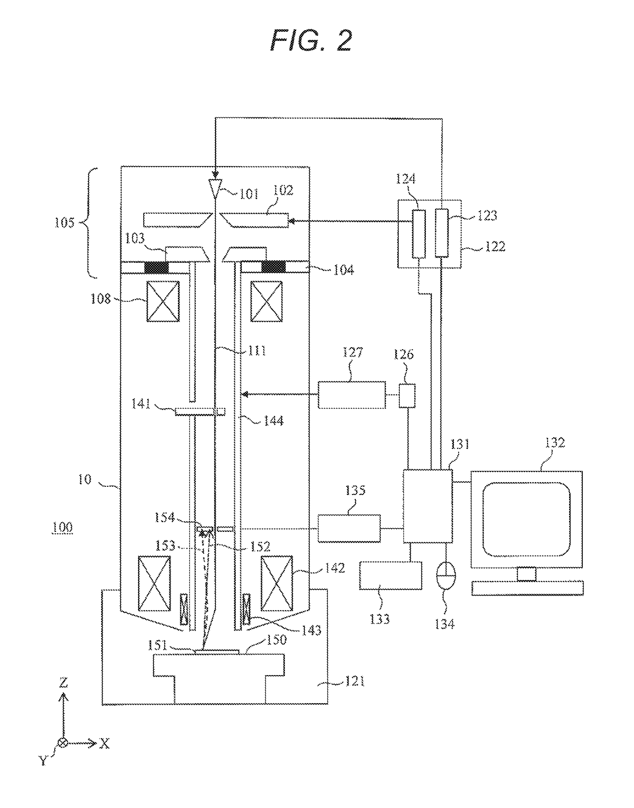
[0041]FIG. 2 illustrates an example of an entire structure of a scanning electron microscope 100 according to the present example. The scanning electron microscope 100 includes a lens tube (column) 10, a sample chamber 121, various power sources, and a control unit. As the various power sources described above, for example, a power source unit 122 (accelerating voltage power source 123 and extracting voltage power source 124) and a booster voltage power source 126 are prepared. The accelerating voltage power source 123 is connected to an electron source 101, the extracting voltage power source 124 is connected to an extracting electrode 102, and the booster voltage power source 1.26 is connected to an anode electrode 103 and a booster electrode 144 via a booster control substrate 127. The control unit includes control a microcomputer / control PC 131, a monitor display 132, a keyboard 133, a mouse 134, and a detection cont...

second example

(2) SECOND EXAMPLE

[0062](2-1) Device structure

[0063]FIG. 4 illustrates a device structure of an electron source and therearound that form a scanning electron microscope according to the present example. In FIG. 4, the parts that correspond to FIG. 1 are given the same reference numerals. One difference between FIG. 4 and FIG. 1 is that, in FIG. 4, an outer periphery of an insulator 109 is directly fixed to an inner wall surface of a lens tube (column) 10 over the entire circumference, and as a result, independent two vacuum chambers are provided. That is, in a scanning electron microscope according to the present example, a vacuum chamber 105A (including an electron source 101) that defines a space at an upstream side with respect to an extracting electrode 102 and a vacuum chamber 105B (including an anode electrode 103) that defines a space at a downstream side with respect to the extracting electrode 102 are independently provided.

[0064]Another difference between FIG. 4 and FIG. 1...

third example

(3) THIRD EXAMPLE

[0066]While a technique to efficiently exhaust the gas 114 generated by collision of the secondary electron 113 with the insulator 104A from the vacuum chamber has been described in the first and the second examples described above, a structure that can prevent generation of the gas 114 will be described in the present example.

(3-1) Device structure

[0067]FIG. 5 illustrates a device structure of an electron source and therearound that form a scanning electron microscope according to the present example. In FIG. 5, the parts that correspond to FIG. 1 are given the same reference numerals. That is, in the present example, a structure including both an electron source 101 and an anode electrode 103 in one vacuum chamber 105 is assumed. A difference between FIG. 5 and FIG. 1 is an attaching structure of an insulator 117 and the anode electrode 103 to an insulating flange 118 of FIG. 5.

[0068]In FIG. 1, the insulating flange 104 and the insulator 104A are integrally formed...


PUM


Abstract

The purpose of the present invention is to be able to acquire high-resolution images in a scanning electron microscope using a combination of a cold cathode (CFE) electron source and a boosting process, even at low accelerating voltage enhancing the current stability of the CFE electron source. A configuration in which a CFE electron source (101), an anode electrode (103) at positive (+) potential, and an insulator (104) for isolating the anode electrode (103) from ground potential are accommodated within a single vacuum chamber (105), and an ion pump (106) and a non-evaporable getter (NEG) pump (107) are connected to the vacuum chamber (105), is employed.

Description

TECHNICAL FIELD[0001]The present invention relates to a scanning electron microscope with a combination of a CFE electron source and a boosting process.BACKGROUND ART[0002]PTL 1 discloses a boosting process (a process in which primary electron beam is caused to pass in a SEM column with high accelerating voltage with a sample kept at ground potential and to be decelerated to ground potential immediately before passing an objective lens). A boosting process can realize, with low accelerating voltage, resolution much higher than a case where a single out-lens objective lens in which magnetic field is not immersed on a sample is used. Note that, in a commercial SEM with a boosting process, a schottky electron source (SE electron source) is mainly used.[0003]PTLs 2 and 3 disclose a cold cathode (CFE: cold field-emission) electron source in which the electron source is not always heated. The current stability (10% / min) of the CFE electron source is extremely worse than that of the SE ele...

Claims


Application Information

Patent Timeline
IPC IPC(8): H01J37/073H01J37/18H01J37/28
CPCH01J37/073H01J37/18H01J2237/2806H01J2237/06341H01J37/28H01J2237/022H01J2237/1825
Inventor AGEMURA, TOSHIHIDESASAKI, MASASHIKOBAYASHI, DAISUKESATO, SHUNSUKE
Owner HITACHI HIGH-TECH CORP
Why Eureka
Try Eureka