Pixel structure, display panel, and curved display device

a display panel and pixel technology, applied in static indicating devices, instruments, non-linear optics, etc., can solve the problems of low contrast and uneven brightness, black matrix of lcd panel to shift, light leakage generation, etc., to reduce resistance-capacitance loading (rc loading), and enhance display quality

Active Publication Date: 2017-11-02
AU OPTRONICS CORP
View PDF3 Cites 5 Cited by
  • Summary
  • Abstract
  • Description
  • Claims
  • Application Information

AI Technical Summary

Benefits of technology

[0005]The disclosure provides a pixel structure, a display panel and a curved display device which not only avoid the issues of uneven brightness, uneven contrast and light leakage caused by a displacement between upper and lower substrates, but also reduce resistance-capacitance loading (RC loading), thereby enhancing display quality.

Problems solved by technology

However, after a liquid crystal display (LCD) panel is bent and / or aligned, an upper substrate and a lower substrate of the LCD panel receive different stress and thus are displacement from each other, which may cause a black matrix of the LCD panel to shift.
As such, light leakage is generated due to incorrect inclination of liquid crystal molecule and undesired electric field.
Besides, after the LCD panel is bent, since different stresses are generated at different locations of the LCD panel, the levels of displacement of the upper and lower substrate are also not the same, which additionally causes the issues of low contrast and uneven brightness (Mura).

Method used


Image

  • Pixel structure, display panel, and curved display device
  • Pixel structure, display panel, and curved display device
  • Pixel structure, display panel, and curved display device

Examples


Embodiment Construction

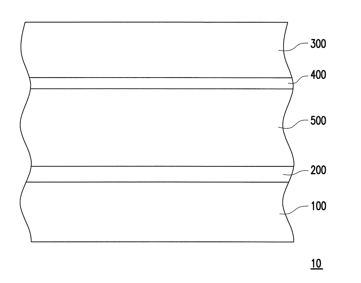
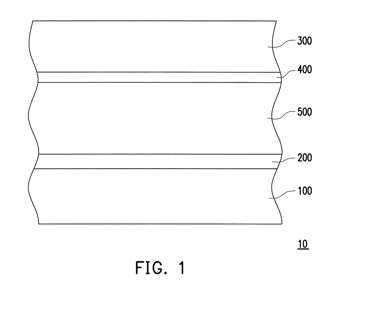
[0021]In the drawings, the thickness of layers, films, panels, regions, etc., are exaggerated for clarity. Like reference numerals designate like elements throughout the specification. It will be understood that when an element such as a layer, film, region, or substrate is referred to as being “on” or “connected to” another element, it can be directly on or connected to the other element or intervening elements may also be present. In contrast, when an element is referred to as being “directly on” or “directly connected to” another element, there are no intervening elements present. As used herein, “connected” may refer to a physical and / or electrical connection.

[0022]“About” or “substantially / approximately” as used herein is inclusive of the stated value and means within an acceptable range of deviation for the particular value as determined by one of ordinary skill in the art, considering the measurement in question and the error associated with measurement of the particular quan...


PUM

PropertyMeasurementUnit
widthaaaaaaaaaa
widthaaaaaaaaaa
width Wdaaaaaaaaaa

Abstract

A pixel structure is provided. The pixel structure has a first substrate, a scan line, a data line, an active device, a pixel electrode, and a conductive strip-shaped pattern. The scan line and the data line are located on the first substrate. The active device is electrically connected to the scan lines and the data line. The pixel electrode is electrically connected to the active device. The conductive strip-shaped pattern is correspondingly disposed over the data line. The conductive strip-shaped pattern has an opening at least partially overlapped with the data line in a vertical projection at the first substrate.

Description

CROSS-REFERENCE TO RELATED APPLICATION[0001]This application claims the priority benefit of Taiwan application serial no. 105113054, filed on Apr. 27, 2016. The entirety of the above-mentioned patent application is hereby incorporated by reference herein and made a part of this specification.BACKGROUND OF THE DISCLOSUREField of Disclosure[0002]The present disclosure relates to a pixel structure, especially to a display panel using the same and a curved display device.Description of Related Art[0003]With the advancement of science and technology, the technology of displays is also continuously developed. Accordingly, light and compact flat-panel displays (FPD) have gradually replaced conventional cathode Ray Tube (CRT) displays. Nowadays, due to the flat-panel displays have the advantages of light weight, compact volume, and slim size, the flat-panel displays are further adopted to be disposed on non-flat surfaces of buildings or electronic equipment. In order to fit the non-flat sur...

Claims


Application Information

Patent Timeline
Patent Type & Authority Applications(United States)
IPC IPC(8): G02F1/1362G02F1/1368G09G3/36
CPCG02F1/136286G02F1/1368G02F1/136209G02F2201/123G09G3/3648G09G2320/0233G09G2300/0439G02F1/134309G02F1/133707
Inventor WANG, JIA-HONGHSU, YA-LING
Owner AU OPTRONICS CORP
Why Eureka
Try Eureka