Fabrication of a vertical fin field effect transistor (vertical finfet) with a self-aligned gate and fin edges

a technology of vertical fin and field effect transistor, which is applied in the direction of basic electric elements, electrical equipment, semiconductor devices, etc., can solve the problems of difficult formation of individual components and electrical contacts

Active Publication Date: 2017-12-14
IBM CORP
View PDF5 Cites 25 Cited by
  • Summary
  • Abstract
  • Description
  • Claims
  • Application Information

AI Technical Summary

Problems solved by technology

With ever decreasing device dimensions, forming the individual components and electrical contacts become more difficult.

Method used


Image

  • Fabrication of a vertical fin field effect transistor (vertical finfet) with a self-aligned gate and fin edges
  • Fabrication of a vertical fin field effect transistor (vertical finfet) with a self-aligned gate and fin edges
  • Fabrication of a vertical fin field effect transistor (vertical finfet) with a self-aligned gate and fin edges

Examples


Embodiment Construction

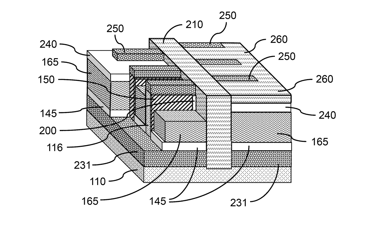
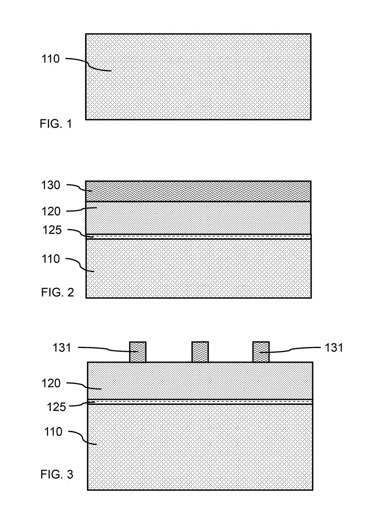
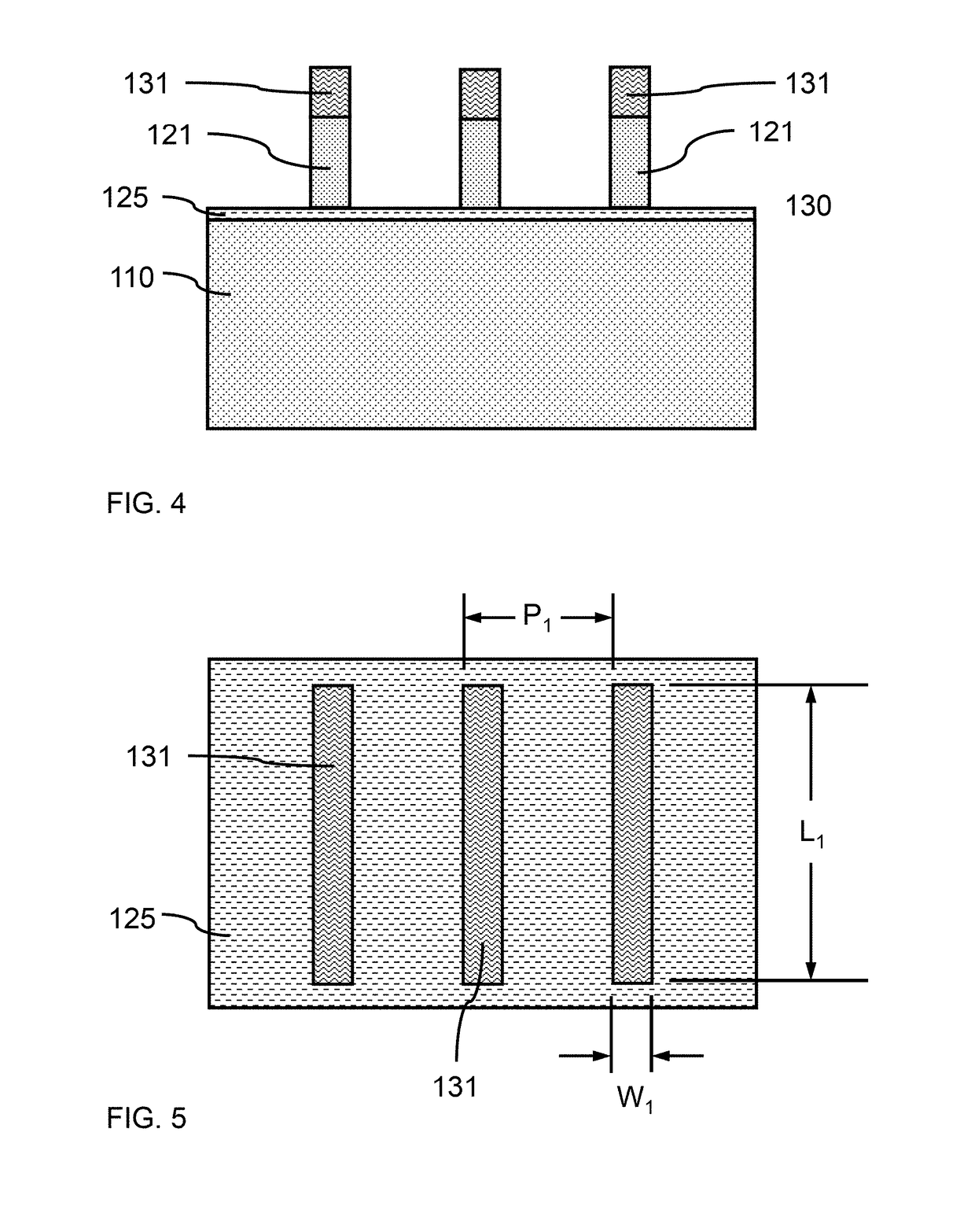
[0037]Principles and embodiments of the present disclosure relate generally to controlling feature locations, dimensions, and inter-feature pitch by reducing or avoiding variations in feature placement through the self-alignment of a fin trench and doped layer. Self-alignment is a process in which control of the placement / formation of device components or features is not limited by the tolerance of control on the positioning of a lithography mask. A device component (e.g., a spacer) or feature (e.g., doped region) may be located through control of feature widths and / or layer thicknesses, or avoidance of sequential mask positionings that may introduce cumulative placement errors.

[0038]For each lithography step, a lithography mask is aligned with features already present on a substrate, and the location of future fabricated features may also be taken into account. The continued reduction in feature sizes has made this alignment more and more difficult. Two such features implemented in...


PUM


Abstract

A method of forming a vertical fin field effect transistor with a self-aligned gate structure, comprising forming a plurality of vertical fins on a substrate, forming gate dielectric layers on opposite sidewalls of each vertical fin, forming a gate fill layer between the vertical fins, forming a fin-cut mask layer on the gate fill layer, forming one or more fin-cut mask trench(es) in the fin-cut mask layer, and removing portions of the gate fill layer and vertical fins not covered by the fin-cut mask layer to form one or more fin trench(es), and two or more vertical fin segments from each of the plurality of vertical fins, having a separation distance, D1, between two vertical fin segments.

Description

BACKGROUNDTechnical Field[0001]The present invention generally relates to self-aligned gate and fin edge, and more particularly to an approach to reduce the dimension between neighboring fin ends to increase device density by cutting the gate and fin concurrently.Description of the Related Art[0002]A Field Effect Transistor (FET) typically has a source, a channel, and a drain, where current flows from the source to the drain, and a gate that controls the flow of current through the channel. Field Effect Transistors (FETs) can have a variety of different structures, for example, FETs have been fabricated with the source, channel, and drain formed in the substrate material itself, where the current flows horizontally (i.e., in the plane of the substrate), and finFETs have been formed with the channel extending outward from the substrate, but where the current also flows horizontally from a source to a drain. The channel for the finFET can be an upright slab of thin rectangular Si, com...

Claims


Application Information

Patent Timeline
Patent Type & Authority Applications(United States)
IPC IPC(8): H01L29/66H01L29/423H01L29/40H01L21/3065H01L21/225H01L29/78H01L21/02H01L21/308
CPCH01L29/66666H01L21/2254H01L21/02129H01L21/02271H01L21/3086H01L29/7827H01L29/4238H01L29/42356H01L29/401H01L21/3065H01L21/3081H01L29/66742H01L29/78642H01L29/66795
Inventor CHENG, KANGGUOMIAO, XINXU, WENYUZHANG, CHEN
Owner IBM CORP
Why Eureka
Try Eureka