Internal crack detecting method and internal crack detecting apparatus

a crack detection and internal crack technology, applied in the direction of semiconductor/solid-state device testing/measurement, image enhancement, instruments, etc., can solve the problem of difficult to clearly detect the cracks generated in the substrate, and achieve the effect of clearly detecting the cracks generated in the workpi

Active Publication Date: 2017-12-28
DISCO CORP
View PDF4 Cites 9 Cited by
  • Summary
  • Abstract
  • Description
  • Claims
  • Application Information

AI Technical Summary

Benefits of technology

[0008]It is therefore an object of the present invention to provide an internal cr

Problems solved by technology

Accordingly, it is difficult to clearly de

Method used


Image

  • Internal crack detecting method and internal crack detecting apparatus
  • Internal crack detecting method and internal crack detecting apparatus
  • Internal crack detecting method and internal crack detecting apparatus

Examples


Embodiment Construction

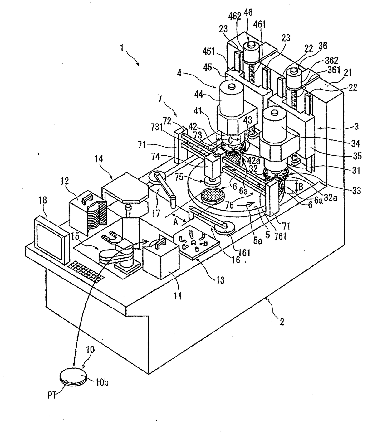
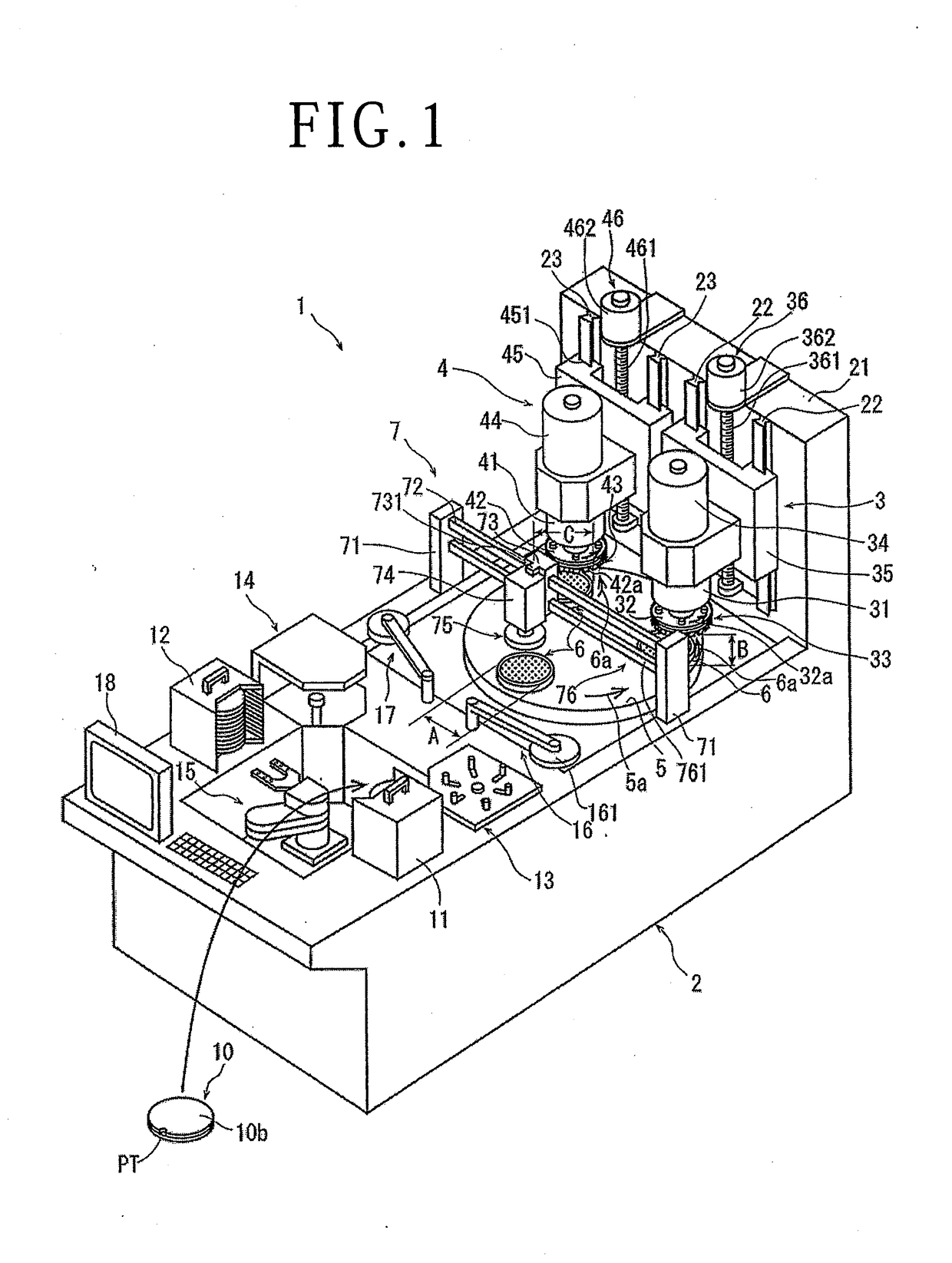
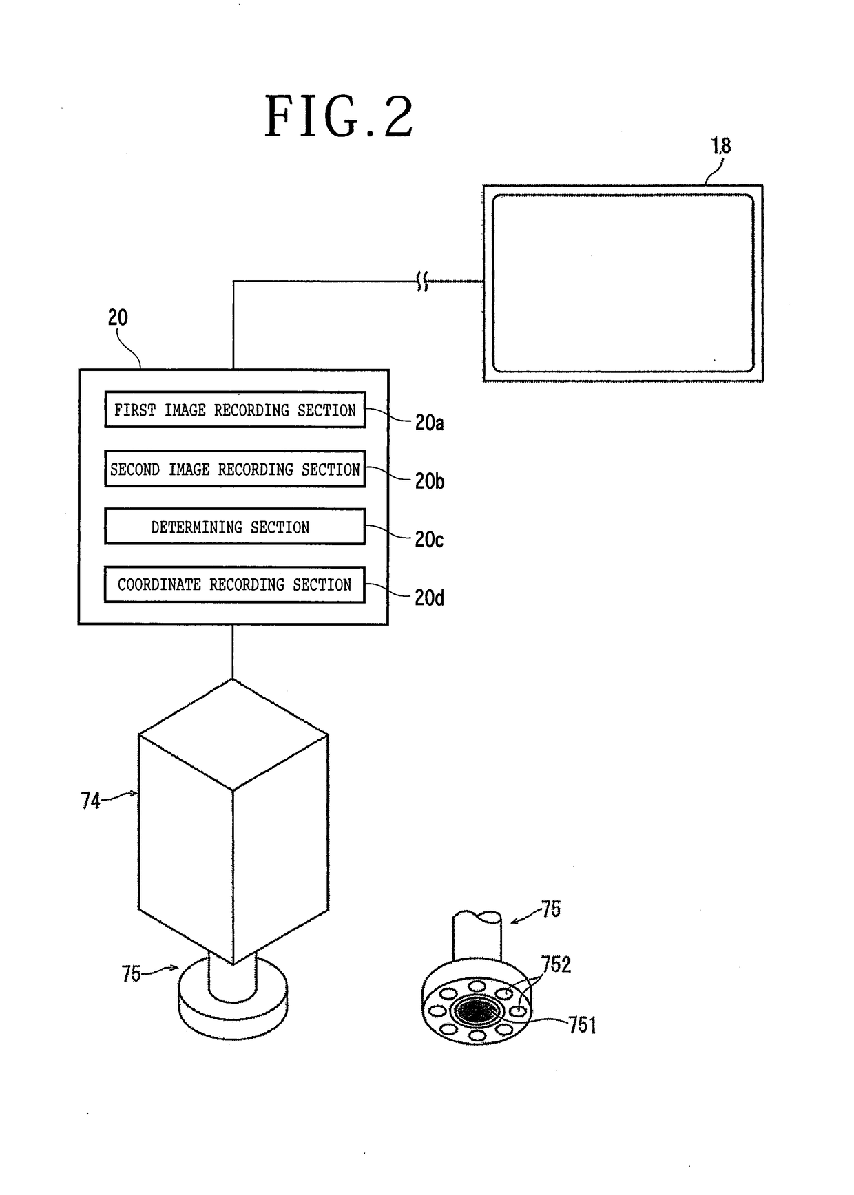
[0021]A preferred embodiment of the internal crack detecting method according to the present invention and the detecting apparatus for performing the detecting method will now be described in detail with reference to the attached drawings. FIG. 1 is a general perspective view of a grinding apparatus 1 including the internal crack detecting apparatus for performing the internal crack detecting method according to the present invention.

[0022]The grinding apparatus 1 shown in FIG. 1 includes a substantially boxlike base housing 2. A stationary support plate 21 projects upward from the upper surface of the base housing 2 at its rear end (at a right upper end as viewed in FIG. 1). Two pairs of guide rails 22, 22 and 23, 23 are provided on the front surface of the stationary support plate 21 so as to extend in a vertical direction. A coarse grinding unit 3 as coarse grinding means is vertically movably mounted on the pair of guide rails 22, 22, and a finish grinding unit 4 as finish grind...


PUM


Abstract

A method for detecting an internal crack in a wafer includes a first image recording step of applying near infrared light having a transmission wavelength to a reference wafer having the same configuration as a target wafer to be subjected to the detection of the internal crack, thereby obtaining a first image of the reference wafer having no internal crack and then recording the first image, a processing step of processing the target wafer, a second image recording step of applying the near infrared light to the target wafer, thereby obtaining a second image of the processed target wafer and then recording the second image, and an internal crack detecting step of removing the same image information between the first image and the second image from the second image to obtain a residual image, thereby detecting the residual image as the internal crack in the target wafer.

Description

BACKGROUND OF THE INVENTION[0001]Field of the Invention[0002]The present invention relates to a method and apparatus for detecting an internal crack generated in processing a workpiece.[0003]Description of the Related Art[0004]A plurality of devices such as integrated circuits (ICs) and large-scale integrations (LSIs) are formed on the front side of a substrate so as to be separated by a plurality of crossing division lines, thus forming a wafer having the plural devices on the front side. The back side of this wafer is ground by a grinding apparatus to reduce the thickness of the wafer. Thereafter, the wafer is divided along the division lines into individual device chips by using a dicing apparatus (see Japanese Patent Laid-open No. 2010-123823, for example) or a laser processing apparatus (see Japanese Patent Laid-open No. 2011-033383, for example). The device chips thus obtained are used in electrical equipment such as mobile phones and personal computers.[0005]In the step of st...

Claims


Application Information

Patent Timeline
IPC IPC(8): G01N21/95H01L21/66G01N21/3563
CPCG01N21/9505G01N21/3563G01B2210/50G01N21/9501G01N2021/3568H01L22/12G01B11/002G06T7/001G01B2210/48G06T2207/10048G06T2207/30148G01N21/956G01N2021/8887
Inventor TAKEDA, NOBORUMORIKAZU, HIROSHI
Owner DISCO CORP
Why Eureka
Try Eureka