

Titanium silicide formation in a narrow source-drain contact
a technology of source-drain contact and titanium silicide, which is applied in the direction of semiconductor devices, semiconductor/solid-state device details, electrical equipment, etc., can solve the problems of reducing the performance of devices, materials and/or processes that were once standard, and may provide unpredictable results or cease to work altogether
- Summary
- Abstract
- Description
- Claims
- Application Information
AI Technical Summary
Benefits of technology
Problems solved by technology
Method used
Image

Examples
example embodiment # 1
Example Embodiment #1
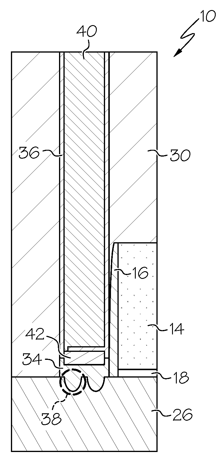
[0031]Referring now to FIGS. 4A-C, a forming of a narrow source-drain contact 40 in the device of FIG. 2 is shown according to an embodiment of the present invention. As shown, titanium liner 34 is deposited on the bottom and (optionally) on the walls of contact trench 32, as shown in FIG. 4A. This depositing of titanium liner 34 in contact trench 32 can be performed using a PVD process (bottom only) or an ALD process (bottom and walls). Then, an x-metal layer 42 is deposited over titanium liner 34 on substantially an entirety of the bottom and (optionally) walls of contact trench 32. As with titanium liner 34, x-metal layer 42 can be deposited in contact trench 32 using a PVD process (bottom only) or an ALD process (bottom and walls). However, it should be understood that x-metal layer 42 is usually deposited on the walls of contact trench 32 only in cases in which titanium liner 34 has previously been deposited on the walls of contact trench 32.
[0032]Then, as ...
example embodiment # 2
Example Embodiment #2
[0033]Referring now to FIGS. 5A-B and 6A-C, a forming of a narrow source-drain contact 40 in the device of FIG. 2 is shown according to an embodiment of the present invention. As shown in FIG. 5A, titanium liner 34 is deposited in contact trench 32, covering substantially an entirety of the bottom and walls of the contact trench. This depositing of titanium liner 34 in contact trench 32 can be performed using an ALD process to cover both the bottom and walls of contact trench 32. Then, as shown in FIG. 5B, x-metal layer 42 is deposited over titanium liner 34 on substantially an entirety of the bottom of contact trench 32. In contrast to titanium liner 34, x-metal layer 42 is deposited in contact trench 32 using a PVD process so that there is no deposit of x-metal on the wall of contact trench 32.
[0034]Then, as shown in FIG. 6A, titanium nitride liner 36 can be formed by nitriding a portion of titanium liner 34 previously deposited on the walls of contact trench ...
example embodiment # 3
Example Embodiment #3
[0035]Referring now to FIGS. 5A-B and 7A-B, a forming of a narrow source-drain contact 40 in the device of FIG. 2 is shown according to an embodiment of the present invention. As in the previous example, titanium liner 34 is deposited in contact trench 32, covering substantially an entirety of the bottom and walls of the contact trench, as shown in FIG. 5A. This depositing of titanium liner 34 in contact trench 32 can be performed using an ALD process to cover both the bottom and walls of contact trench 32. Then, as shown in FIG. 5B, x-metal layer 42 is deposited over titanium liner 34 on substantially an entirety of the bottom of contact trench 32. In contrast to titanium liner 34, x-metal layer 42 is deposited in contact trench 32 using a PVD process so that there is no deposit of x-metal on the walls of contact trench 32.
[0036]Then, as shown in FIG. 7A, titanium nitride liner 36 can be formed by nitriding a portion of titanium liner 34 previously deposited on...
PUM
| Property | Measurement | Unit |
|---|---|---|
| width | aaaaa | aaaaa |
| contrast | aaaaa | aaaaa |
| contrast | aaaaa | aaaaa |
Abstract
Description
Claims
Application Information