Otp memory with high data security

Active Publication Date: 2018-01-04
ATTOPSEMI TECH CO LTD
View PDF4 Cites 30 Cited by
  • Summary
  • Abstract
  • Description
  • Claims
  • Application Information

AI Technical Summary

Benefits of technology

The patent describes a way to make programmable resistive devices using junction diodes as program selectors. These devices can be made in standard CMOS logic processes, which makes them smaller and cheaper. The use of P+ / N well diodes allows for the fabrication of PMOS devices using the same well that houses the sources or drains of PMOS and NMOS devices. This reduces cell size and special processing requirements, making it ideal for embedded applications. Overall, this technology simplifies the process of making programmable resistive devices and makes them more accessible for various applications.

Problems solved by technology

As a result, the cell size of an electrical fuse using silicided polysilicon tends to be very large.
Though this technology can reduce the PCM cell size to only 6.8F2 (F stands for feature size), the diode requires very complicated process steps, such as Selective Epitaxial Growth (SEG), to fabricate, which would be very costly for embedded PCM applications.
The fuse elements 80, 84 in FIGS. 3(a) and 3(b) are relatively large structures which makes them unsuitable for some applications.

Method used


Image

  • Otp memory with high data security
  • Otp memory with high data security
  • Otp memory with high data security

Examples


Embodiment Construction

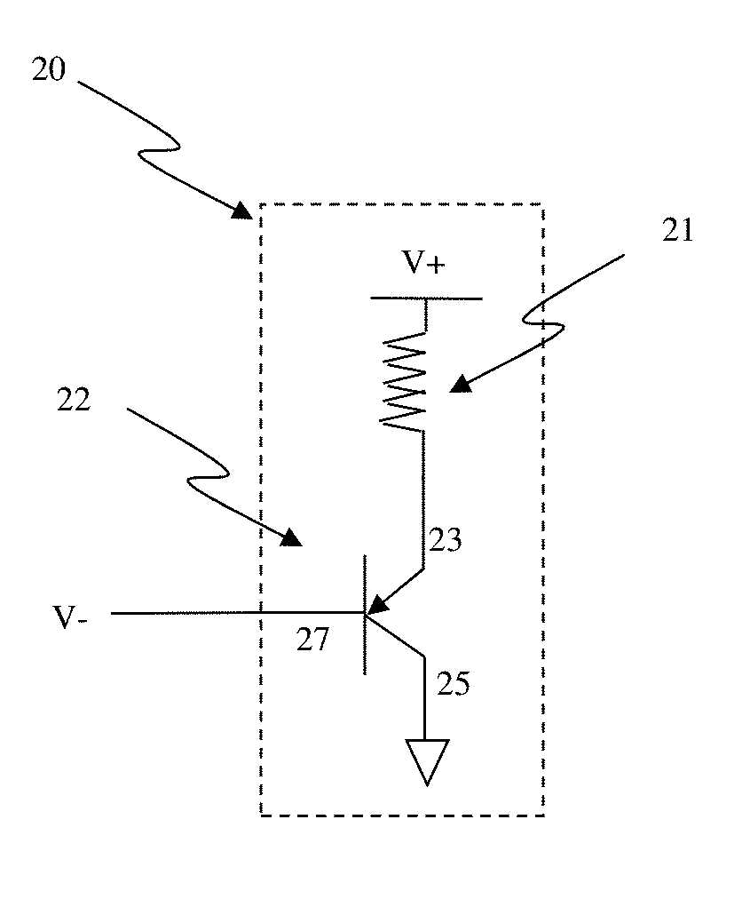
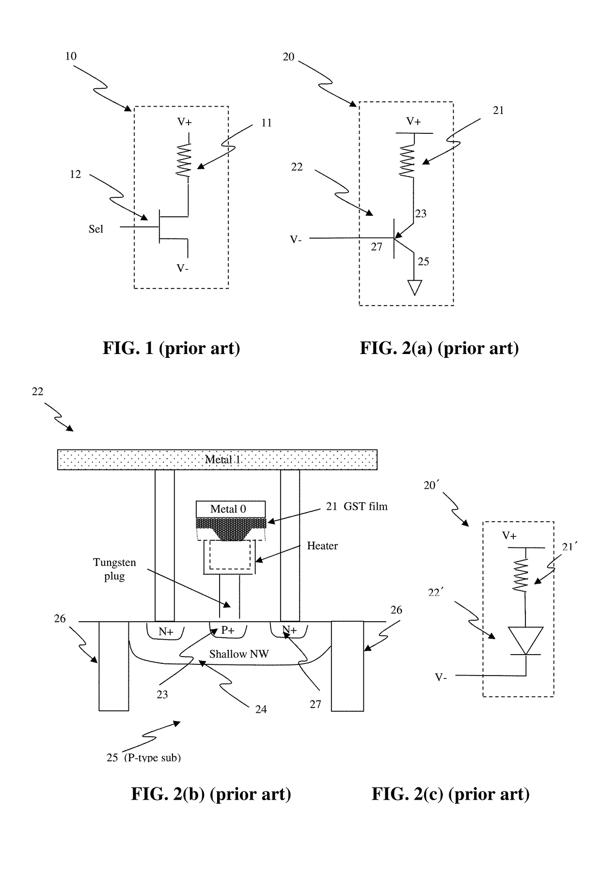
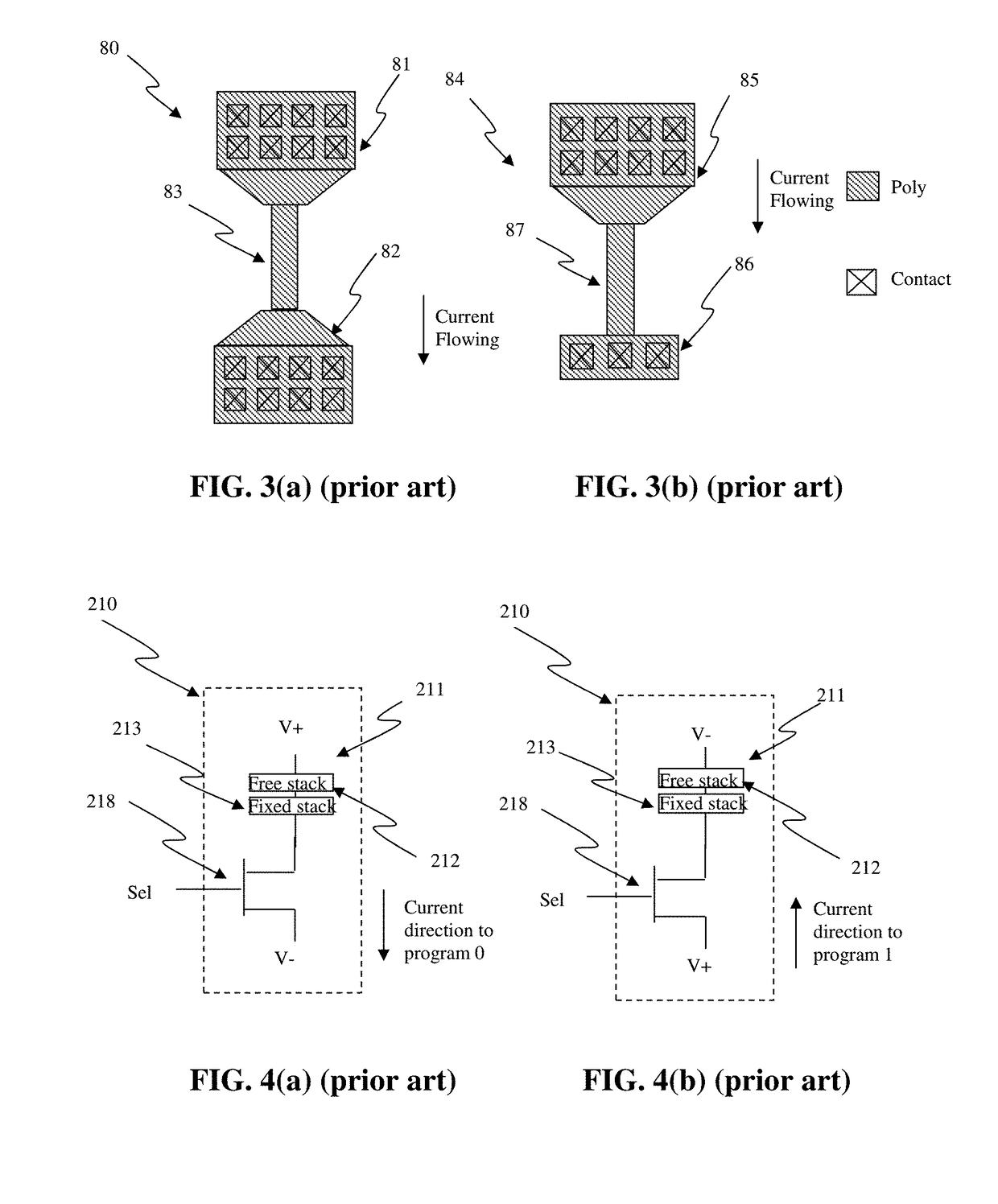
[0165]Embodiments disclosed herein use a P+ / N well junction diode as program selector for a programmable resistive device. The diode can comprise P+ and N+ active regions on an N well. Since the P+ and N+ active regions and N well are readily available in standard CMOS logic processes, these devices can be formed in an efficient and cost effective manner. For standard Silicon-On-Insulator (SOI), FinFET, or similar technologies, isolated active regions can be used to construct diodes as program selectors or as programmable resistive elements. The programmable resistive device can also be included within an electronic system.

[0166]In one or more embodiments, junction diodes can be fabricated with standard CMOS logic processes and can be used as program selectors for One-Time Programmable (OTP) devices. The OTP devices can include electrical fuses are programmable elements. Examples of electrical fuses include interconnect fuse, contact / via fuse, contact / via anti-fuse, gate-oxide break...


PUM


Abstract

A method of programming electrical fuses reliably is disclosed. If a programming current exceeds a critical current, disruptive mechanisms such as rupture, thermal runaway, decomposition, or melt, can be a dominant programming mechanism such that programming is not be very reliable. Advantageously, by controlled programming where programming current is maintained below the critical current, electromigration can be the sole programming mechanism and, as a result, programming can be deterministic and very reliable. In this method, fuses can be programmed in multiple shots with progressive resistance changes to determine a lower bound that all fuses can be programmed satisfactorily and an upper bound that at least one fuse can be determined failed. If programming within the lower and upper bounds, defects due to programming can be almost zero and, therefore, defects are essentially determined by pre-program defects.

Description

CROSS-REFERENCE TO RELATED APPLICATIONS[0001]This application claims priority benefit of U.S. Provisional Patent Application No. 62 / 462,351, filed on Feb. 22, 2017 and entitled “One-Time Programmable Memory,” which is hereby incorporated herein by reference.[0002]This application is also a continuation-in-part of U.S. patent application Ser. No. 15 / 422,266, filed on Feb. 1, 2017 and entitled “Method and Structure for Reliable Electrical Fuse Programming,” which is hereby incorporated herein by reference, which is a continuation of U.S. patent application Ser. No. 14 / 485,696, filed on Sep. 13, 2014 and entitled “Method and Structure for Reliable Electrical Fuse Programming,” which is a continuation-in-part of U.S. patent application Ser. No. 13 / 835,308, filed on Mar. 15, 2013 and entitled “Circuit and System of Using Junction Diode as Program Selector for One-Time Programmable Devices,” which is a continuation of U.S. patent application Ser. No. 13 / 471,704, filed on May 15, 2012 and ...

Claims


Application Information

Patent Timeline
IPC IPC(8): G11C17/16G11C29/02G11C17/18
CPCG11C29/027G11C17/18G11C17/16H10B61/10H10B63/20H10N70/231H10N70/8828H10N70/826G11C7/222
Inventor CHUNG, SHINE C.
Owner ATTOPSEMI TECH CO LTD
Why Eureka
Try Eureka