

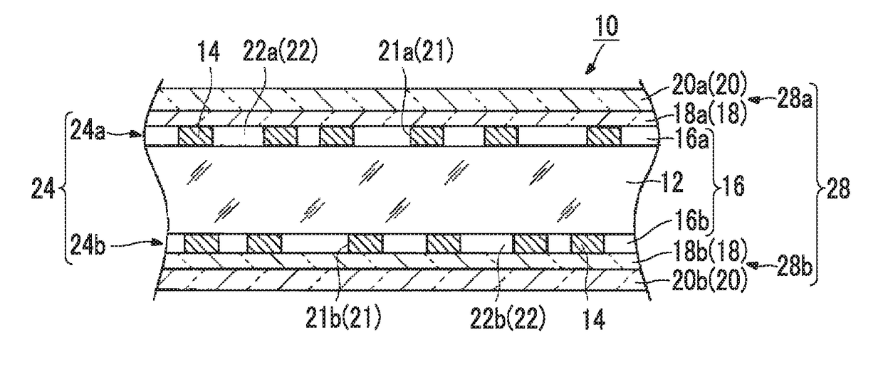
Conductive film, display device having the same, and method of evaluating conductive film
a display device and conductive film technology, applied in the field of conductive film, can solve the problems of difficult control, difficult to greatly improve image quality, and poor noise visibility, and achieve robust image quality, robust image quality, and robust image quality.
- Summary
- Abstract
- Description
- Claims
- Application Information
AI Technical Summary
Benefits of technology
Problems solved by technology
Method used
Image

Examples
experimental example
[0191]Hereinafter, the present invention will be described in detail with reference to an experimental example.
[0192]In the present example, in accordance with the flow of the method of evaluating the conductive film of the present invention shown in FIG. 21, in a manner similar to the above description, an experiment was performed as follows.
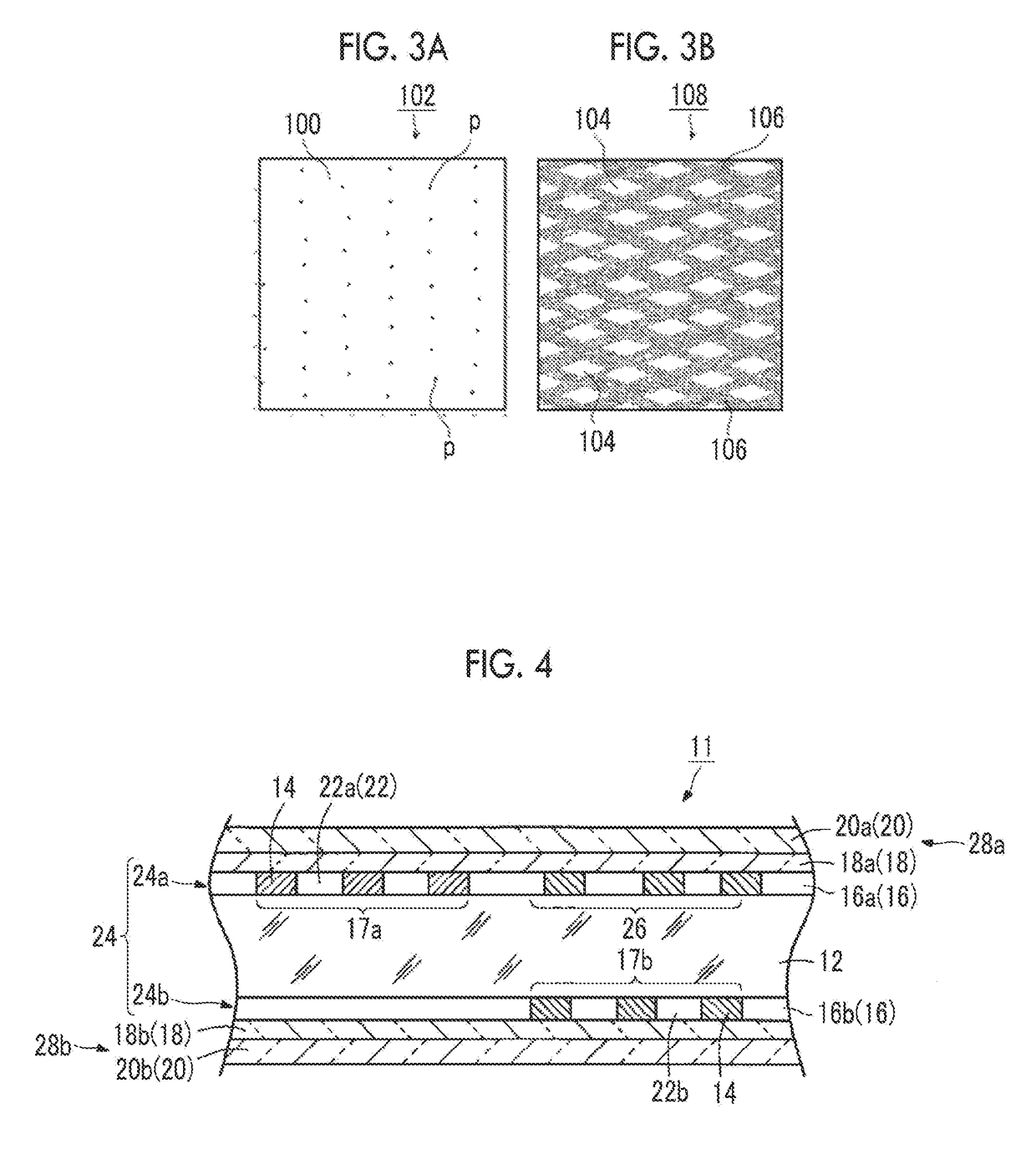
[0193]In accordance with the flow of the method of evaluating the conductive film shown in FIG. 21, 46 kinds of the mesh patterns 1 to 46 are produced, spectrum anisotropy (directivity) of the 46 kinds of the produced mesh patterns was quantified. Table 1 shows the 46 kinds of the produced mesh patterns 1 to 46.
[0194]A brief overview of the mesh patterns 1 to 46 shown in Table 1 was as follows.
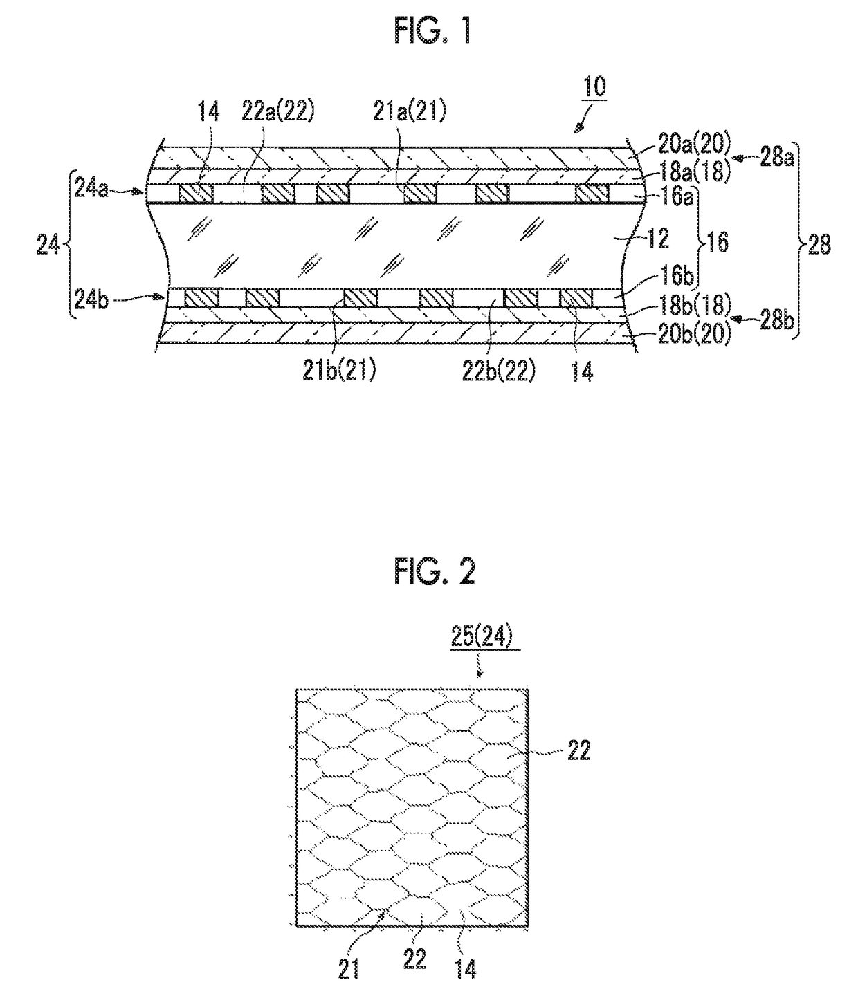
[0195]The mesh patterns 1 to 9 were Voronoi random patterns each of which was formed of Voronoi polygons, and respectively have average pitches in a range of 200 μm to 300 μm and line widths in a range of 2 μm to 6 μm.
[0196]The mesh patterns 10 and 11 wer...
PUM
| Property | Measurement | Unit |
|---|---|---|
| transparent | aaaaa | aaaaa |
| width | aaaaa | aaaaa |
| width | aaaaa | aaaaa |
Abstract
Description
Claims
Application Information