
Using MLC flash as SLC by writing dummy data

a technology of mlc flash and dummy data, applied in the field of nonvolatile storage, can solve the problem of actual shifts in the charge stored in the cell, and achieve the effect of improving the reliability of data storag

Active Publication Date: 2009-06-09
WESTERN DIGITAL ISRAEL LTD
View PDF23 Cites 37 Cited by
  • Summary
  • Abstract
  • Description
  • Claims
  • Application Information

AI Technical Summary

Benefits of technology

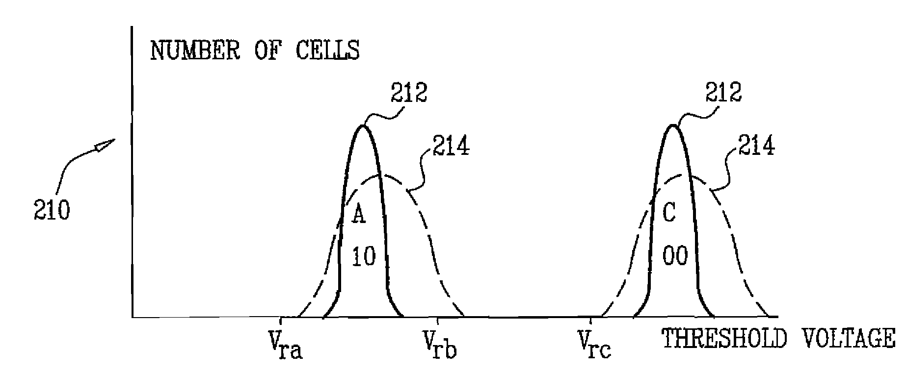
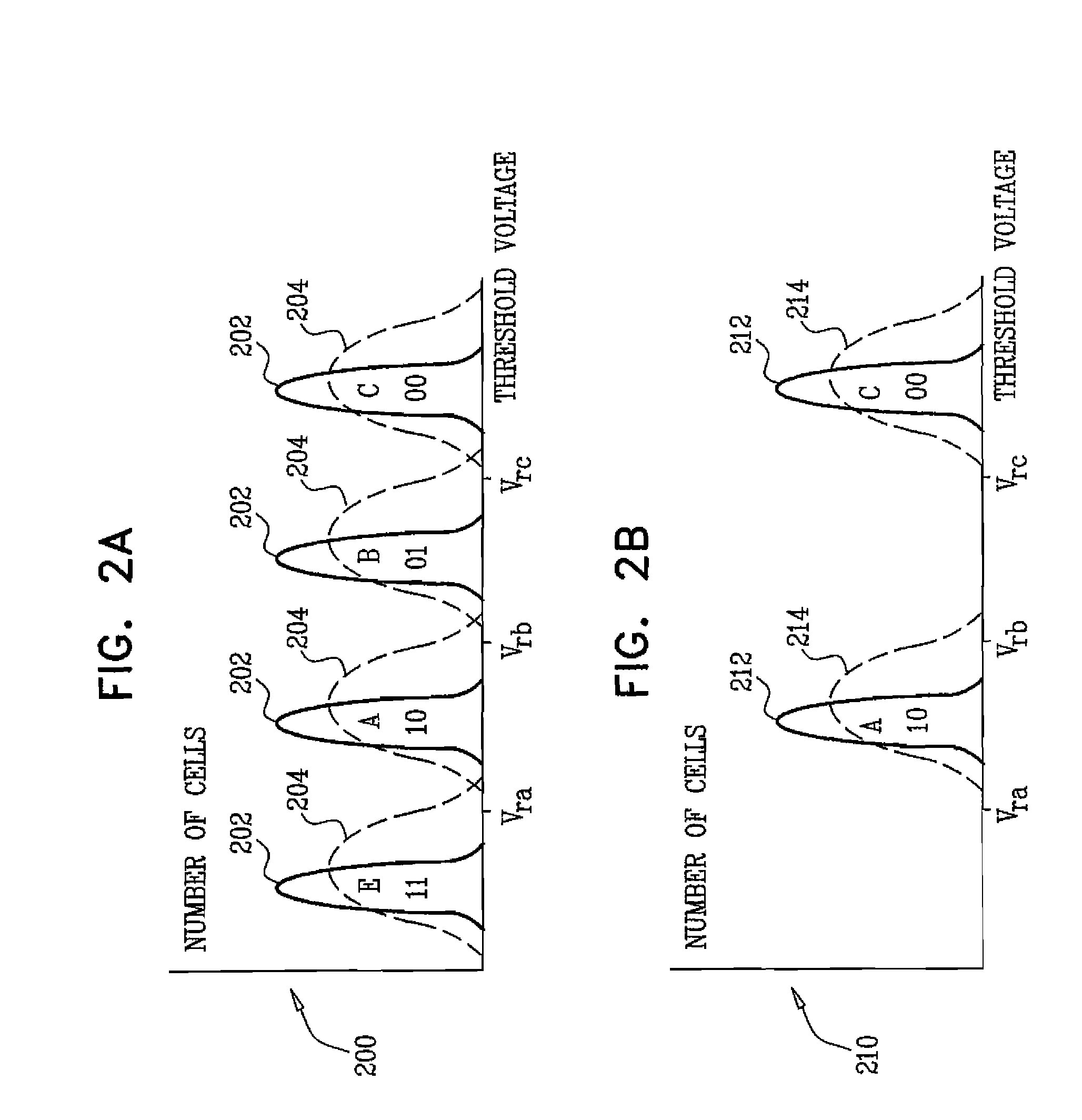
[0008]Embodiments of the present invention provide apparatus and methods for storing input data in a group of cells in an MLC memory device at a density that is lower than the designed density of the device. Dummy data is stored to one or more bits of all cells in the group, thereby limiting the number of bits in each cell to which actual input data may be written. The dummy data is independent of the input data and typically has a uniform bit value that is chosen so as to maximize a difference between voltage states assumed by cells in the group. The increased difference between voltage states may improve the reliability of data storage.
[0013]In disclosed embodiments, the dummy data include a uniform bit value that is stored to at least one of the bits in the first set in all of the cells in the group. Typically, the cells in the memory array have a predetermined set of voltage states, and the dummy data are selected so as to maximize a distance between the voltage states resulting from storing the dummy data and writing the input data.

Problems solved by technology

In flash memory, actual shifts in the charge stored in a cell can occur when reading, programming or erasing a neighboring cell, due to electrical coupling between cells, as well as due to leakage of charge through the oxide insulating the gate of the cell over long periods of storage time.

Method used


Image

  • Using MLC flash as SLC by writing dummy data
  • Using MLC flash as SLC by writing dummy data
  • Using MLC flash as SLC by writing dummy data

Examples


Embodiment Construction

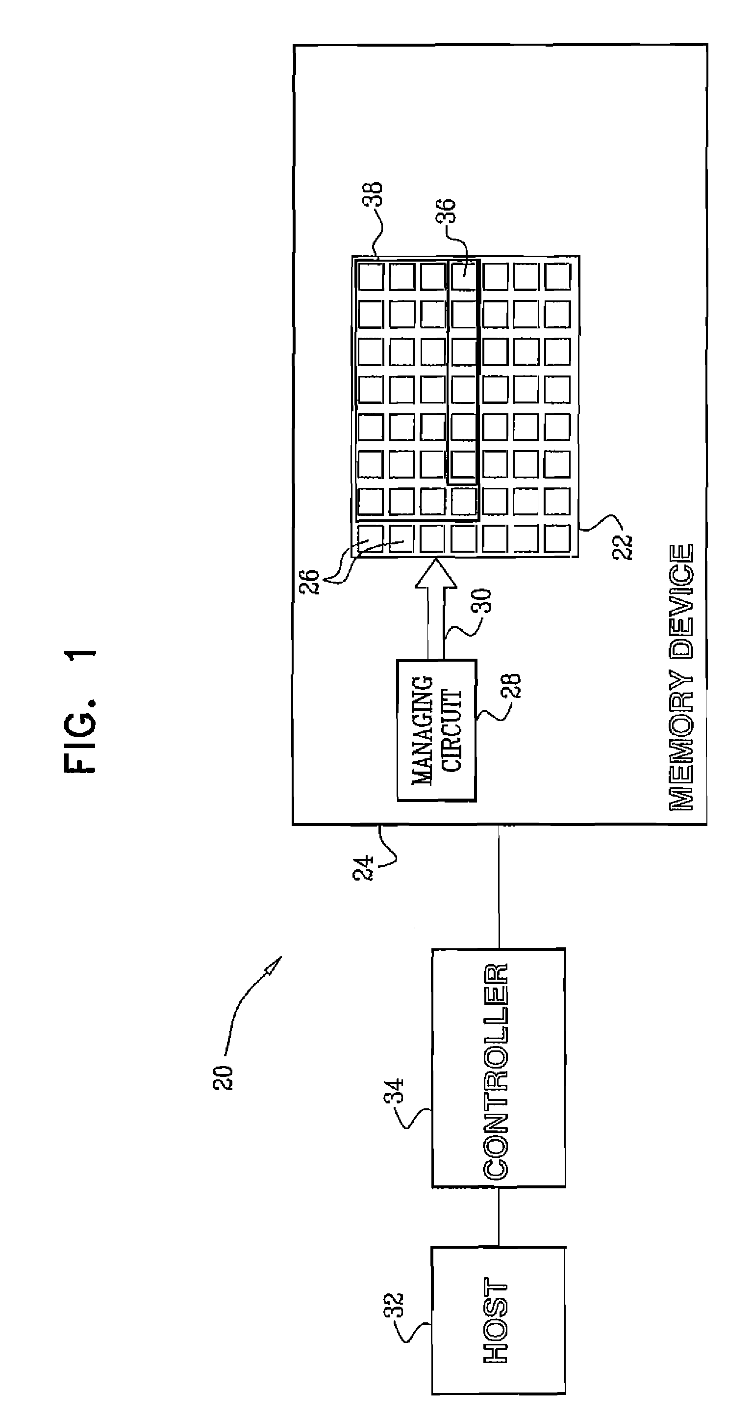
[0028]Reference is now made to FIG. 1, which is a block diagram that schematically illustrates a system 20 for storing data to a portion of a memory cell array 22 of an MLC memory device 24, in accordance with an embodiment of the present invention. Exemplary embodiments of the present invention described hereinbelow refer to non-volatile memory, and specifically flash memory, but principles of the present invention may be applied mutatis mutandis to other types of MLC memory.

[0029]Memory cell array 22 comprises memory cells 26, which are designed to retain four or more distinct voltage states, such that at least two bits of data may be stored to each cell. In the exemplary embodiment that is described hereinbelow, cells 26 have a two bit density, so that one bit of each cell is the less significant bit (LSB) and the other bit is the more significant bit (MSB). Alternatively, the principles of the present invention may be applied to memory devices that are designed to store three or...


PUM


Abstract

A method for storing data includes designating, in a memory array including cells configured for writing a first number of bits per cell, a group of the cells to which input data are to be written at a second number of bits per cell, smaller than the first number. Dummy data that are independent of the input data are stored in a first set of one or more bits of the cells in the group. The input data are written to a second set of at least one other bit of the cells in the group.

Description

FIELD OF THE INVENTION[0001]The present invention relates generally to technology for non-volatile storage.BACKGROUND OF THE INVENTION[0002]Non-volatile semiconductor memory devices are widely used as memory storage in computers and other electronic appliances. In Single-Level Cell (SLC) memory devices, a charge-retaining gate in each memory cell of the device is designed to retain a charge, such that the gate can be in either a charged state or an erased state. Each memory cell may therefore store a single bit of data, one state representing a logical “1” (typically associated with the erased state) and the other state a logical “0” (typically associated with the charged state).[0003]In Multi-Level Cell (MLC) memory, the gate in each memory cell may be set to four or more different voltage states, or ranges, thereby providing a data density of two or more data bits per cell. MLC memory is described, for example, in U.S. Pat. No. 5,043,940, to Harari, and in U.S. Pat. No. 5,172,338,...

Claims


Application Information

Patent Timeline
Patent Type & Authority Patents(United States)
IPC IPC(8): G11C16/04
CPCG11C11/5628G11C2211/5641
Inventor LASSER, MENAHEM
Owner WESTERN DIGITAL ISRAEL LTD
Learn More