Electrical contact pair and connector terminal pair
a technology of connector terminals and contact points, which is applied in the direction of coupling contact members, etc., can solve the problems of poor wear resistance, decrease in the connection reliability of a pair of connector terminals, and significant wear due to adhesion, so as to improve the wear resistance of sliding and reduce the amount of sliding wear. , the effect of small friction coefficien
- Summary
- Abstract
- Description
- Claims
- Application Information
AI Technical Summary
Benefits of technology
Problems solved by technology
Method used
Image
Examples
embodiment 1
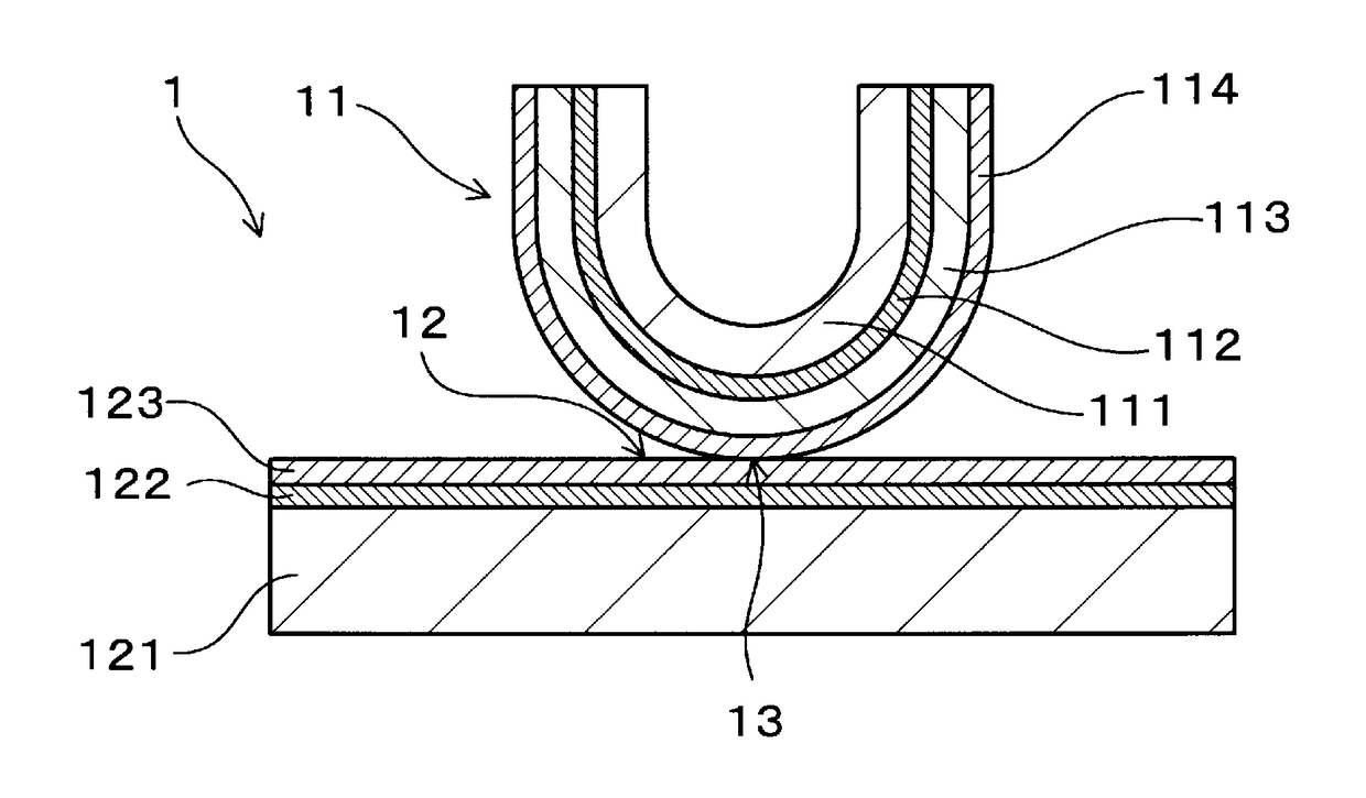
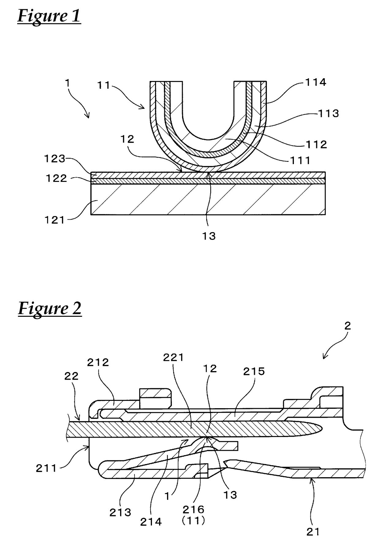
[0039]An electrical contact pair and a connector terminal pair according to Embodiment 1 will be described with reference to FIGS. 1 and 2. As shown in FIG. 1, an electrical contact pair 1 of the present embodiment includes a first electrical contact 11, a second electrical contact 12, and a contact portion 13. The first electrical contact 11 includes, a first conductive base material 111, an Ag—Sn alloy layer 113 that is laminated on a surface of the first conductive base material 111 with Ni layer 112 and / or a Ni alloy layer interposed therebetween, and a first AG layer 114 that is laminated on a surface of the Ag—Sn alloy layer 113. In the first electrical contact 11, the first AG layer 114 is exposed as the outermost surface. The second electrical contact 12 a second conductive base material 121, and a second AG layer 123 that is laminated on a surface of the second conductive base material 121 with a Ni layer 122 and / or a Ni alloy layer interposed therebetween. Note that in the...
embodiment 2
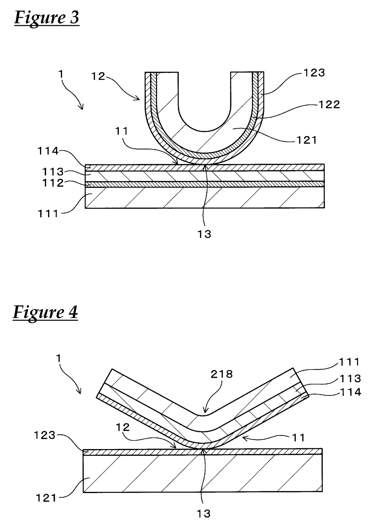
[0051]An electrical contact pair and connector terminals according to Embodiment 2 will be described with reference to FIG. 3. As shown in FIG. 3, according to the present embodiment, a second electrical contact 12 of an electrical contact pair 1 has a protruding shape. Specifically, the second electrical contact 12 includes a protruding shape second conductive base material 121, a Ni alloy layer 122 that is laminated on a surface of the second conductive base material 121, and a second AG layer 123 that is laminated on a surface of the Ni alloy layer 122. The second conductive base material 121 is made of copper or a copper alloy, and has a thickness of 250 μm. The Ni alloy layer 122 has a thickness of 1 μm. The second AG layer 123 has a thickness of 1 μm.
[0052]On the other hand, in the present embodiment, a first electrical contact 11 has the shape of a plate that comes into electrical contact with the top of the protruding second electrical contact 12. Specifically, the first ele...
reference example 3
[0055]An electrical contact pair and a connector terminal according to Reference Example 3 will be described with reference to FIGS. 4 to 6. As shown in FIG. 4, a first electrical contact 11 of the present embodiment includes a bent portion 218. Specifically, the first electrical contact 11 includes a first conductive base material 111 that is folded to have the bent portion 218, an Ag—Sn alloy layer 113 that is laminated on a surface of the first conductive base material 111, and a first AG layer 114 that is laminated on a surface of the Ag—Sn alloy layer 113. The first conductive base material 111 is made of aluminum or an aluminum alloy, and has a thickness of 250 μm. The Ag—Sn alloy layer 113 has a thickness of 4 μm. The first AG layer 114 has a thickness of 1 μm.
[0056]On the other hand, in the present embodiment, a second electrical contact 12 has the shape of a plate that comes into electrical contact with the bent portion 218 of the first electrical contact 11. Specifically, ...
PUM
 Abstract
Description
Claims
Application Information


