
Eureka
For R&D, Eureka makes reading and utilizing patents & technical documents easy.
Eureka AIR
Designed for self-driven R&D workflows. Generate viable solutions, solve complex R&D challenges, empower your innovation with AI.

Eureka Materials
Designed for material experts only. Revolutionize your material R&D, from search, analyze, to developing new materials.

TechResearch
Generate reliable direction feasibility study reports for your R&D in just a few steps.

TechSeek
Discover and master advanced knowledge NOW. Basics, ideas, possibilities, all at once.

TechMind
As an expert in R&D Theories, TechMind can generates customized viable solutions instantly.

TechRisk
Analyze your overall solution with one click, know your potential R&D risks in advance.

TechMonitor
Get weekly tech updates, stay abreast of the latest tech innovations and key insights.
Sensing device
- Summary
- Abstract
- Description
- Claims
- Application Information
AI Technical Summary
Benefits of technology
Problems solved by technology
Method used
Image

Examples
Embodiment Construction
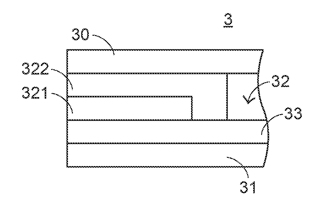
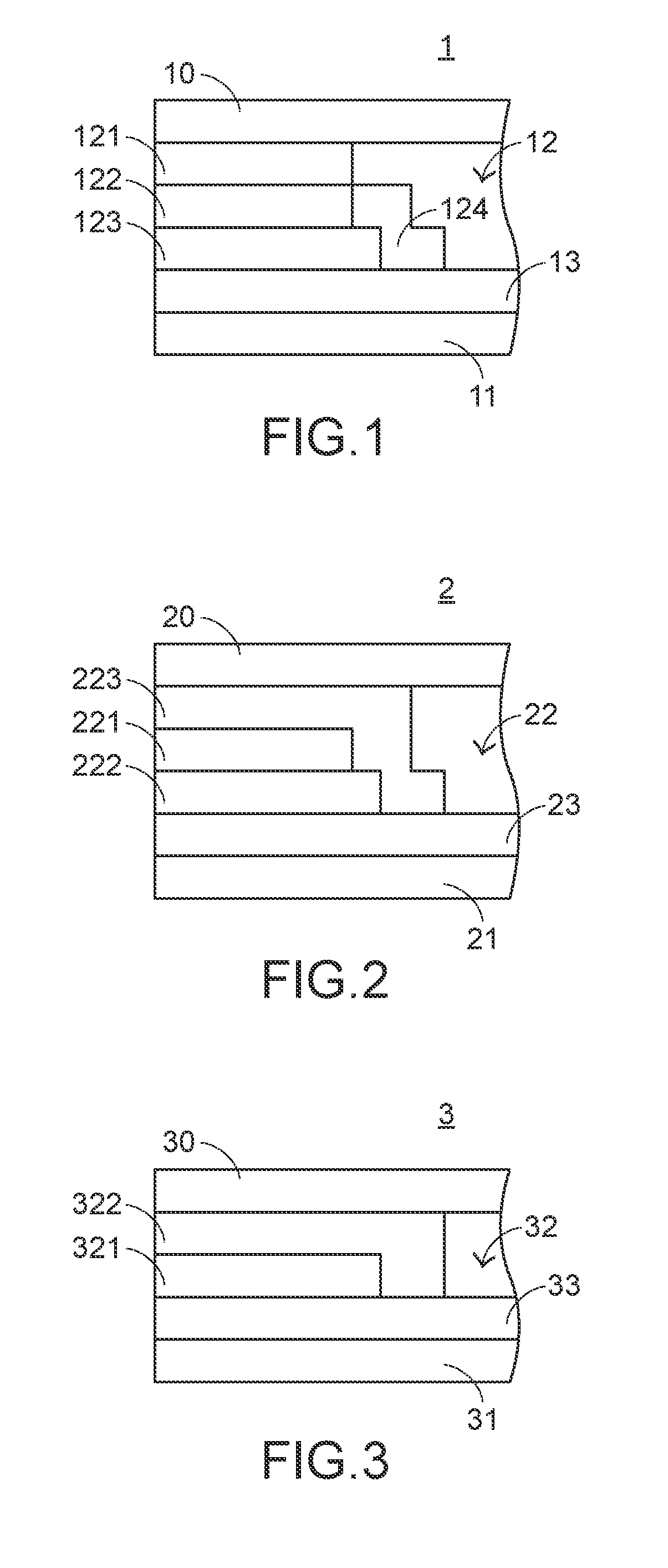
[0014]The present invention provides a sensing device, to solve a conventional technical problem. Referring to FIG. 2, FIG. 2 is a schematic structural diagram of a sensing device of the present invention in a first preferred embodiment. The sensing device 2 can retrieve a surface imaging of an object (which is not shown in the figure), and includes a protective cover 20, a transmitting electrode module 21, a receiving electrode module 22, and a substrate 23. The receiving electrode module 22 includes a receiving electrode layer 221, an insulating plate 222, and a conductive circuit layer 223. These components are sequentially the protective cover 20, the conductive circuit layer 223, the receiving electrode layer 221, the insulating plate 222, the substrate 23, and the transmitting electrode module 21 from top to bottom. The conductive circuit layer 223 covers the receiving electrode layer 221, the insulating plate 222, and a part of the substrate 23. In the preferred embodiment, t...
PUM
 Abstract
Description
Claims
Application Information
 - R&D Engineer
- R&D Manager
- IP Professional
- Industry Leading Data Capabilities
- Powerful AI technology
- Patent DNA Extraction
Browse by: Latest US Patents, China's latest patents, Technical Efficacy Thesaurus, Application Domain, Technology Topic, Popular Technical Reports.
© 2024 PatSnap. All rights reserved.Legal|Privacy policy|Modern Slavery Act Transparency Statement|Sitemap|About US| Contact US: help@patsnap.com