Bit line sense amplifier for inhibiting increase of offset voltage and method for fabricating the same

a technology of offset voltage and amplifier, which is applied in the direction of instruments, mechanical equipment, cylinders, etc., can solve the problems of reducing the sensitivity of the bit line sense amplifier, and achieve the effect of improving the sensitivity of the sense amplifier, improving the dram characteristics, and improving the arrangement and connection of the devices

Active Publication Date: 2005-09-29
SK HYNIX INC
View PDF2 Cites 9 Cited by
  • Summary
  • Abstract
  • Description
  • Claims
  • Application Information

AI Technical Summary

Benefits of technology

[0019] Accordingly, it is an object of the present invention to inhibit increase of an offset voltage due to inconsistency of electrical characteristics which results from difference in location of devices by improving arrangement and connection of the devices in a bit line sense amplifier, thereby improving sensitivity of the sense amplifier and characteristics of the DRAM.

Problems solved by technology

As described above, since the offset voltage of the bit line sense amplifier adds to change of characteristics of the symmetrical devices in the arrangement of the devices in the conventional bit line sense amplifier, the offset voltage becomes larger, thereby reducing sensitivity of the bit line sense amplifier.

Method used


Image

  • Bit line sense amplifier for inhibiting increase of offset voltage and method for fabricating the same
  • Bit line sense amplifier for inhibiting increase of offset voltage and method for fabricating the same
  • Bit line sense amplifier for inhibiting increase of offset voltage and method for fabricating the same

Examples


Embodiment Construction

[0031] The present invention will be described in detail with reference to the accompanying drawings.

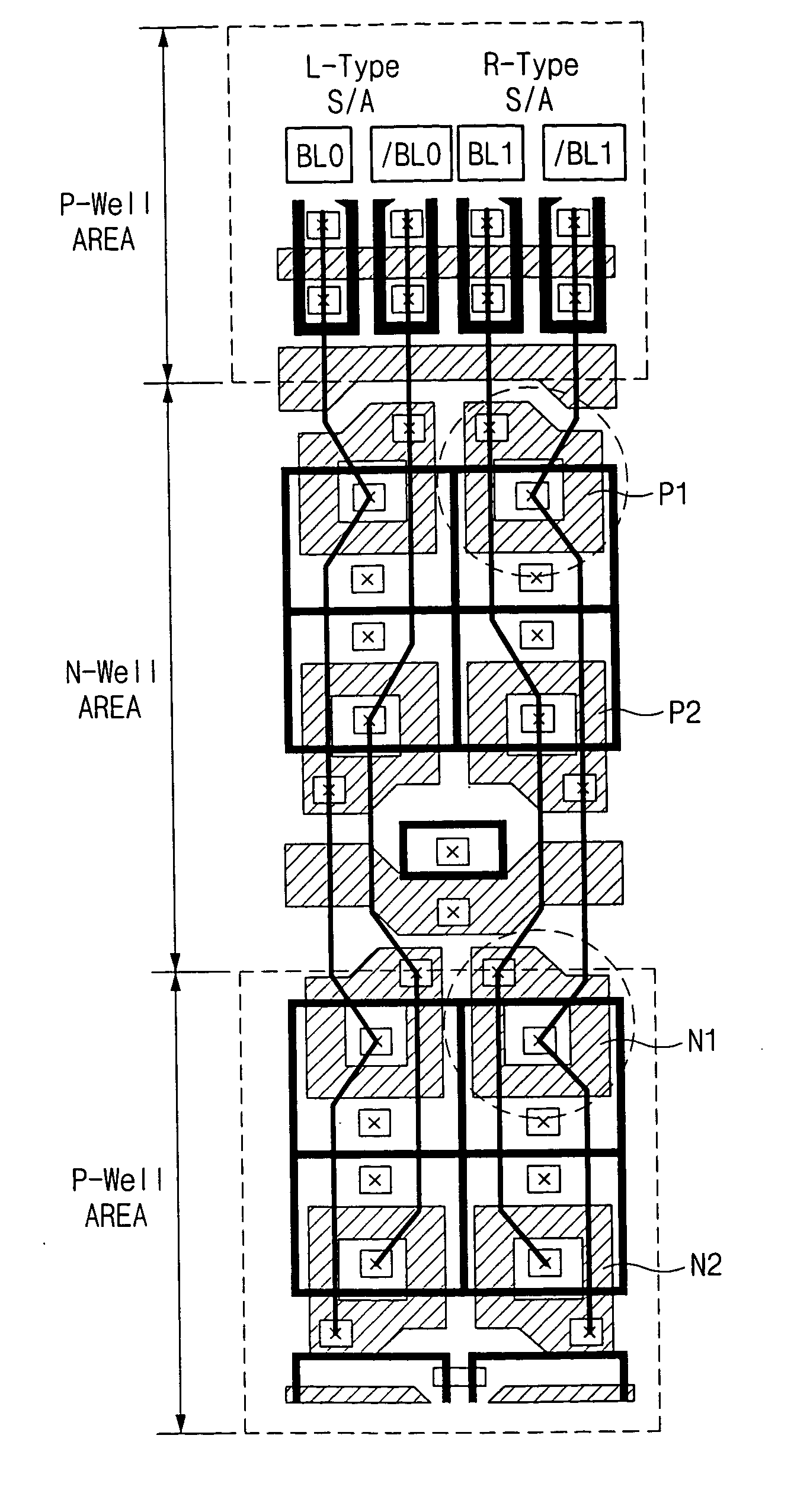
[0032]FIG. 5 is a circuit layout diagram illustrating a connection state of a bit line sense amplifier according to an embodiment of the present invention.

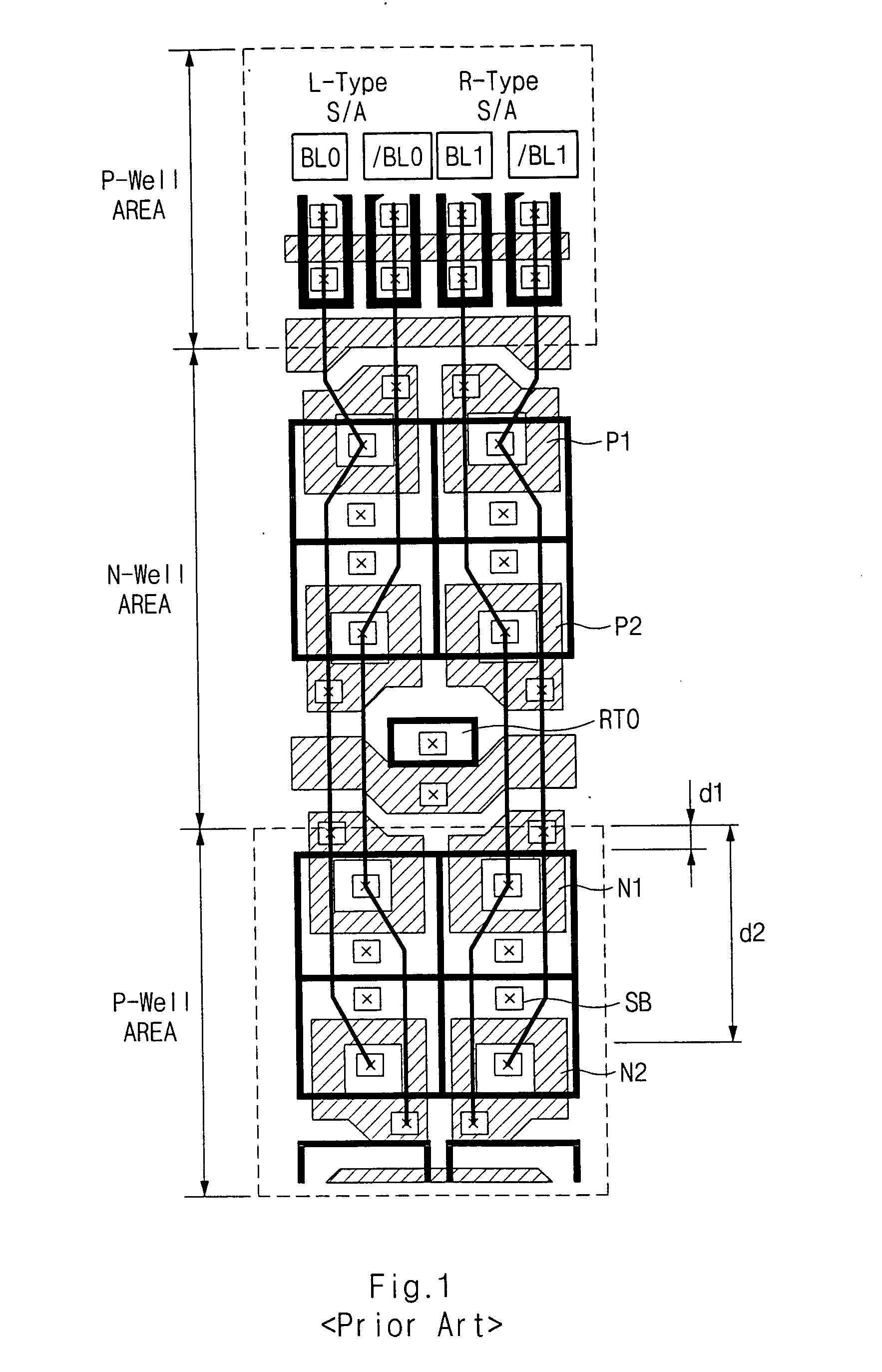
[0033] Referring to FIG. 5, while PMOS transistors P1 and P2 of a N-well region are the same as those of FIG. 1, FIG. 5 is different from FIG. 1 in arrangement and connection of gates and drains of NMOS transistors N1 and N2 in a P-well region.

[0034] That is, while the bit line BL1 of FIG. 1 is connected to the gate of the NMOS transistor N2 through the drain of the NMOS transistor N1, a bit line BL1 of FIG. 5 is connected to a drain of a NMOS transistor N2 through a gate of a NMOS transistor N1.

[0035] Additionally, while the bit line bar / BL1 of FIG. 1 is connected to the drain of the NMOS transistor N2 through the gate of the NMOS transistor N1, the bit line bar / BL1 of FIG. 5 is connected to a gate of the NMOS transistor N2 ...


PUM


Abstract

A bit line sense amplifier for inhibiting increase of an offset voltage, and a method for fabricating the same are provided. The bit line sense amplifier comprises a plurality of CMOS inverters, which are cross-coupled corresponding to the paired bit lines. Each of the CMOS inverters senses and amplifies a voltage of the paired bit lines. Here, transistors comprised in each inverter are positioned at the same location in a well region where the transistors are formed. As a result, increase of the offset voltage due to inconsistency of electrical characteristics which results from difference in location of devices is inhibited, thereby improving sensitivity of the sense amplifier and characteristics of the DRAM.

Description

BACKGROUND ART [0001] 1. Field of the Invention [0002] The present invention generally relates to a bit line sense amplifier, and more specifically, to a bit line sense amplifier for inhibiting increase of an offset voltage by offsetting an effect due to characteristic inconsistency of devices which results from difference in space location of devices. [0003] 2. Description of the Prior Art [0004] In a DRAM, a sense amplifier as a device for sensing insignificant information stored in a cell and then amplifying the sensed information is positioned in two paired bit lines BL and / BL. However, since the width between the paired bit lines BL and / BL is so narrow that symmetrical NMOS transistors or PMOS transistors are not arranged in parallel but in serial. As a result, the symmetrical NMOS transistors or PMOS transistors which are required to have the same electrical characteristics have relative difference in location to adjacent circuits. [0005]FIG. 1 is a circuit layout diagram il...

Claims


Application Information

Patent Timeline
Patent Type & Authority Applications(United States)
IPC IPC(8): G11C7/06G11C11/4091H01L27/108
CPCG11C7/065H01L27/10897G11C11/4091H10B12/50B21H1/18
Inventor MYOUNG RHO, KWANG
Owner SK HYNIX INC
Why Eureka
Try Eureka