Thin film transistor for electrowetting display device and manufacturing method thereof

An electrowetting display, thin film transistor technology, applied in transistors, semiconductor/solid state device manufacturing, electric solid state devices and other directions, can solve the problems of poor fluidity of oily substances, poor overall display, slow reaction speed, etc. Induction sensitivity, improving product opening rate, and the effect of speeding up the response

Active Publication Date: 2010-04-14
SHENZHEN LAIBAO HI TECH
View PDF0 Cites 9 Cited by
  • Summary
  • Abstract
  • Description
  • Claims
  • Application Information

AI Technical Summary

Problems solved by technology

Due to the difference in principle between liquid crystal display and electrowetting display, if the thin film transistors currently used in liquid crystal display devices are used in electrowetting display devices, the following defects will appear: 1. The aperture ratio is low, and the overall display is not good. Good; 2. Structurally, the level difference of each area is large, and the fluidity of the oily substance in the electrowetting display device is not good, so the reaction speed is slow

Method used


Image

  • Thin film transistor for electrowetting display device and manufacturing method thereof
  • Thin film transistor for electrowetting display device and manufacturing method thereof
  • Thin film transistor for electrowetting display device and manufacturing method thereof

Examples


Embodiment Construction

[0044] In order to make the object, technical solution and advantages of the present invention clearer, the present invention will be further described in detail below in conjunction with the accompanying drawings and embodiments. It should be understood that although the present invention has been described by the embodiments, those skilled in the art know that the present invention has many modifications and changes without departing from the spirit of the present invention, and the specific embodiments described here are only used to explain the present invention, and It is not intended to limit the scope of the invention.

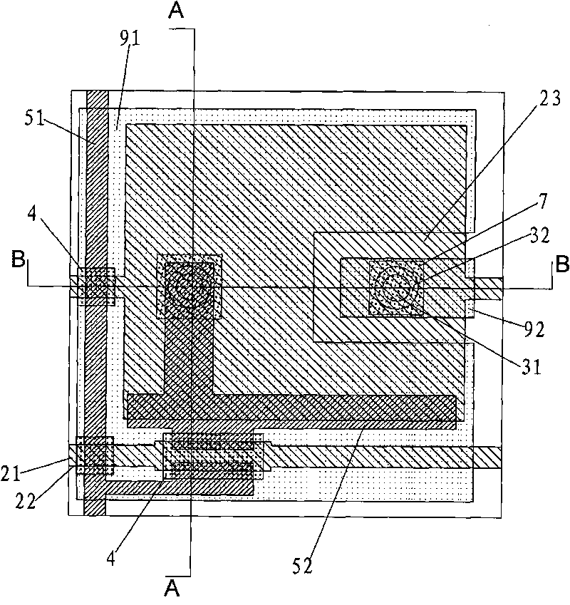
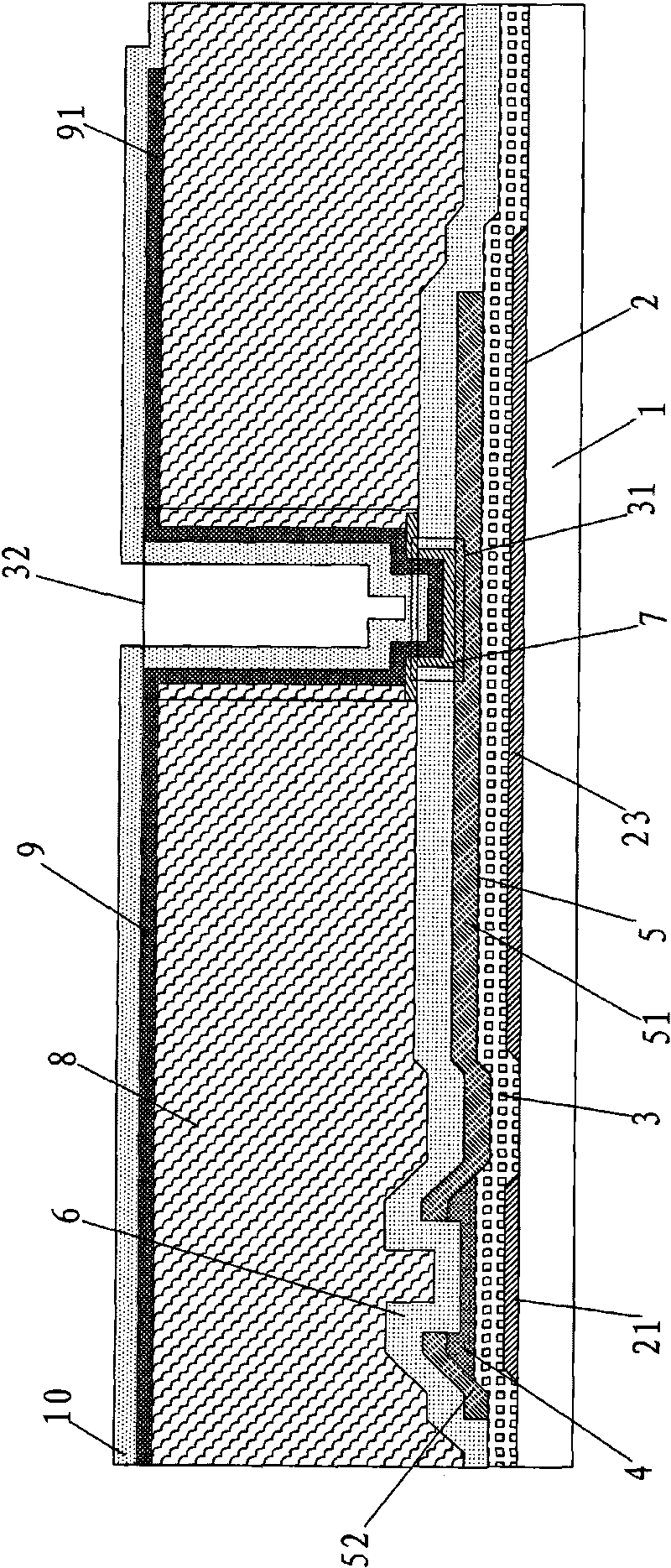
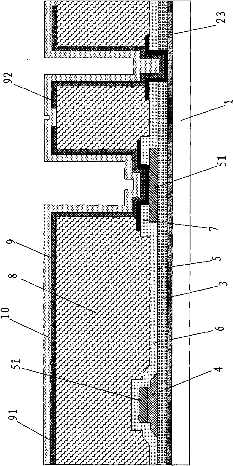
[0045] Please refer to figure 1 , 2, 3, the present invention discloses a thin film transistor for an electrowetting display device, comprising: a substrate 1, a bottom conductive film layer 2, a first insulating film layer 3, a semiconductor amorphous silicon film layer 4, a second Conductive film layer 5, second insulating layer 6, third conductive ...


PUM


Abstract

The invention discloses a thin film transistor for an electrowetting display device and a manufacturing method thereof. The thin film transistor comprises a basal plate, a bottom conducting film layer, a first insulating film layer, a semiconductor amorphous silicon film layer, a second conducting film layer, a second insulating layer, a fourth conducting film layer and an organic leveling film layer; the bottom conducting film layer is arranged on the basal plate; the first insulating film layer is covered above the bottom conducting film layer; the semiconductor amorphous silicon film layer is covered on the first insulating film layer; the second conducting film layer is partially covered on the semiconductor amorphous silicon film layer, and the second layer of the insulating film layer is covered above the first insulating film layer, the semiconductor amorphous silicon film layer and the second conducting film layer; the organic leveling film layer is covered on the second insulating layer; and the fourth conducting film layer is covered on the organic leveling film layer. Compared with the prior art, the invention has the advantages that the reaction speed is improved as the organic leveling film layer is added; a drain electrode and a public electrode are both connected with the same plane by the conducting film layers, therefore, the reaction speed is accelerated; and the opening rate of the product is improved.

Description

technical field [0001] The present invention relates to the field of electrowetting display devices, in particular to a thin film transistor used in an electrowetting display device and a manufacturing method. Background technique [0002] At present, the flat panel display industry is developing rapidly. The mainstream display devices include liquid crystal display devices (LCD). received great attention. [0003] However, both liquid crystal display devices and electrowetting display devices involve thin film transistors. The working principle of the liquid crystal display device is mainly to rely on the liquid crystal in the device to be twisted by the action of the upper and lower electrodes, and then display different graphics through the polarizer attached to the upper and lower electrodes; and the electrowetting display The working principle of the device is mainly: relying on the oily substance in the device, according to the different voltages it receives, it will...

Claims


Application Information

Patent Timeline
Patent Type & Authority Applications(China)
IPC IPC(8): G02B26/02H01L29/786H01L23/528H01L21/336H01L21/768
Inventor 商陆平朱泽力李绍宗
Owner SHENZHEN LAIBAO HI TECH
Why Eureka
Try Eureka