Electronic device

Active Publication Date: 2018-03-01
ROBERT BOSCH GMBH
View PDF0 Cites 2 Cited by
  • Summary
  • Abstract
  • Description
  • Claims
  • Application Information

AI Technical Summary

Benefits of technology

[0009]In an alternative embodiment, the at least one connecting pin formed as the fuse element contacts the housing. In order to prevent damage or to great of mechanical stresses, such a contacting takes place in a resilient manner. This can, for example, be achieved by at least one area portion adjoining the contact point of the at least one connecting pin formed as the fuse element, said area portion being configured in a flexible manner. In the case of connecting pins that are designed wire-shaped, such an implementation is very simple. In the case of a sufficiently long wire section, said section is enabled, when a force is applied transversely to a wire extension, to elastically deform in the direction of the applied force. Thus, the wire section can be an end of the connecting pin or be disposed between two fastened ends of the connecting pin. By virtue of the fact that the wire section and the housing are disposed at an angle in relation to one another, the elastically flexible wire section is pushed away by the housing up to a contact point, which is predetermined for the operation of the electronic device, at the instance of the formation of the contact point, for example during the installation of the electronic device.
[0010]Provision is made in a particular embodiment for the housing to have a bulge projecting into the cavity and the extremely small distance to than be formed at the bulge. In this way, it is not required that the connecting pin provided as the fuse element to have to be designed as the furthest projecting element of the electric and/or electronic circuit. In fact, the advantage results from this embodiment that an arbitrary topology or respectively a multi-sided construction of the electric and/or electronic circuit can occur. By providing the previously mentioned bulge, an accommodation of the housing in the region of the at least one connecting pin formed as the fuse element is accordingly provided in a targeted manner, such that the extremely small distance of the housing to a conductive region of the electric and/or electronic circuit is ensured exactly in said region. In an advantageous manner, a taking into account of the fuse element at an arbitrary position on the circuit carrier is thus facilitated.
[0011]A possible embodiment furthermore provides that the housing comprises at least two housing elements that form the cavity. It is thus conceivable that the one housing element is a cover and the further housing element is a base element that can be sealed by the cover. Furthermore, at least one of the housing elements, for example the cover, is designed as a cast part. In this case, the previously described bulge projecting into the cavity of the housing can easily be implemented as a correspondingly integrally formed dome attachment in the cast part. The dome attachment can have processing surfaces, for example by means of a mechanical removal, such as, for example, by means of a milling procedure. Hence, the extremely small distance can be implemented between the dome attachment and the at least one connecting pin formed as the fuse element in a narrow tolerance range. The same applies to the case of an alternative embodiment, in which one of the housing elements is d

Problems solved by technology

Electrostatic discharges can often damage the electric circuit and/or components of the electric and/or electronic circuit.
At the point in time of the electrostatic di

Method used


Image

  • Electronic device
  • Electronic device
  • Electronic device

Examples


Example

[0018]In the figures, functionally identical components are in each case denoted with the same reference signs.

DETAILED DESCRIPTION

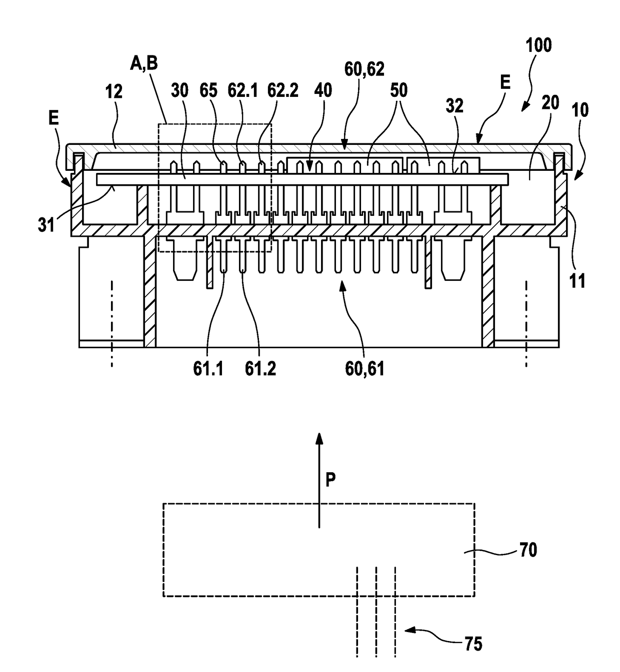
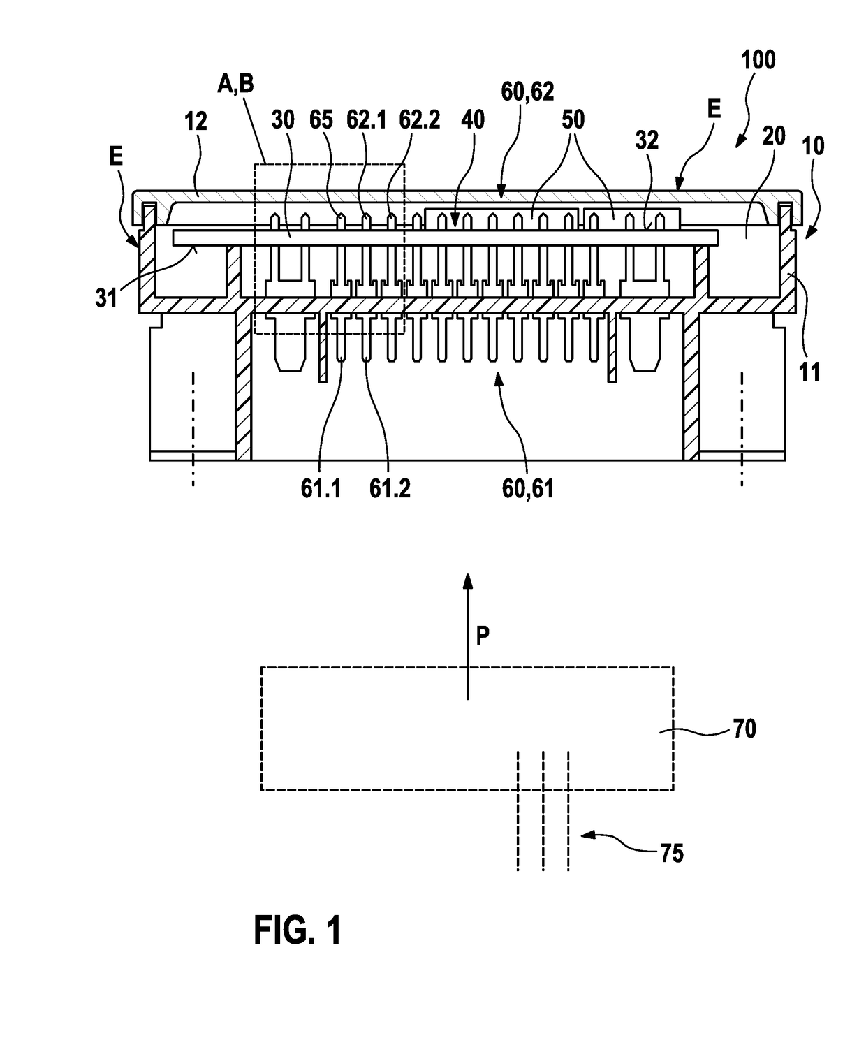
[0019]FIG. 1 shows an electronic device according to the invention in a side cross-sectional view. The electronic device 100 comprises a housing 10, which consists of a base element 11 and a cover 12. The base element 11 is, for example, formed from plastic, in particular as a plastic injection-molded part. The cover 12 is, for example, made from metal, in particular from Al or an Al alloy. The cover is thereby set on the base element 11 and fastened to the same, for example by screws or adhesives. In so doing, a cavity 20 is formed between the cover 12 and the base part 11. A circuit carrier 30 is accommodated within the cavity 20. A conductor path structure is formed (not depicted) on an upper side 32 and / or a lower side 31 of the circuit carrier 30. Furthermore, the circuit carrier 30 is fitted with an electric and / or electronic component 50. The elec...


PUM


Abstract

The invention relates to an electronic device, in particular a control device, having a housing. The housing has a cavity, in which there is arranged a circuit carrier fitted with electric and/or electronic components, forming an electric and/or electronic circuit. Furthermore, the electronic device has a fuse element making contact with the circuit carrier in order to protect the electric and/or electronic circuit against electrostatic discharges. In addition, the electric and/or electronic circuit comprises a plug contact which has connecting pins, and the connecting pins make contact with the circuit carrier. Here, the at least one connecting pin is formed as the fuse element, in that the at least one connecting pin is connected to a ground line. Furthermore, an extremely small distance of the housing from an electrically conductive region of the electronic and/or electronic circuit is provided at a point of the at least one connecting pin formed as a fuse element, by which means, in the event of an electrostatic discharge, a preferred discharge path is formed between the housing and the ground line.

Description

BACKGROUND OF THE INVENTION[0001]The invention relates to an electronic device, in particular a control device, having a housing, which has a cavity, in which there is arranged a circuit carrier fitted with electric and / or electronic components, forming an electric and / or electronic circuit, and having a fuse element making contact with the circuit carrier in order to protect the electric and / or electronic circuit against electrostatic discharges.[0002]Electronic devices comprise electric and / or electronic circuits, which are very sensitive with regard to an electrostatic discharge. An electrostatic discharge can result for a variety of reasons. For example, it is possible that housing parts—for example made from plastic—charge themselves electrostatically. From a certain amount of charge, the electrostatic charge can then jump from the housing onto electrically conductive regions of the electric and / or electronic circuit. It is likewise possible for the electronic device to move in...

Claims


Application Information

Patent Timeline
IPC IPC(8): H05K1/02H02H9/04H05K7/14H01R12/71H01R13/696H01R13/648
CPCH05K1/0259H02H9/04H05K7/1427H01R12/712H01R13/696H01R13/6485H05K5/0047H05K9/0039H05K9/0067
Inventor KUHN, JOCHEN
Owner ROBERT BOSCH GMBH
Why Eureka
Try Eureka