
Eureka
For R&D, Eureka makes reading and utilizing patents & technical documents easy.
Eureka AIR
Designed for self-driven R&D workflows. Generate viable solutions, solve complex R&D challenges, empower your innovation with AI.

Eureka Materials
Designed for material experts only. Revolutionize your material R&D, from search, analyze, to developing new materials.

TechResearch
Generate reliable direction feasibility study reports for your R&D in just a few steps.

TechSeek
Discover and master advanced knowledge NOW. Basics, ideas, possibilities, all at once.

TechMind
As an expert in R&D Theories, TechMind can generates customized viable solutions instantly.

TechRisk
Analyze your overall solution with one click, know your potential R&D risks in advance.

TechMonitor
Get weekly tech updates, stay abreast of the latest tech innovations and key insights.
Wafer and method of processing wafer
- Summary
- Abstract
- Description
- Claims
- Application Information
AI Technical Summary
Benefits of technology
Problems solved by technology
Method used
Image

Examples
Embodiment Construction
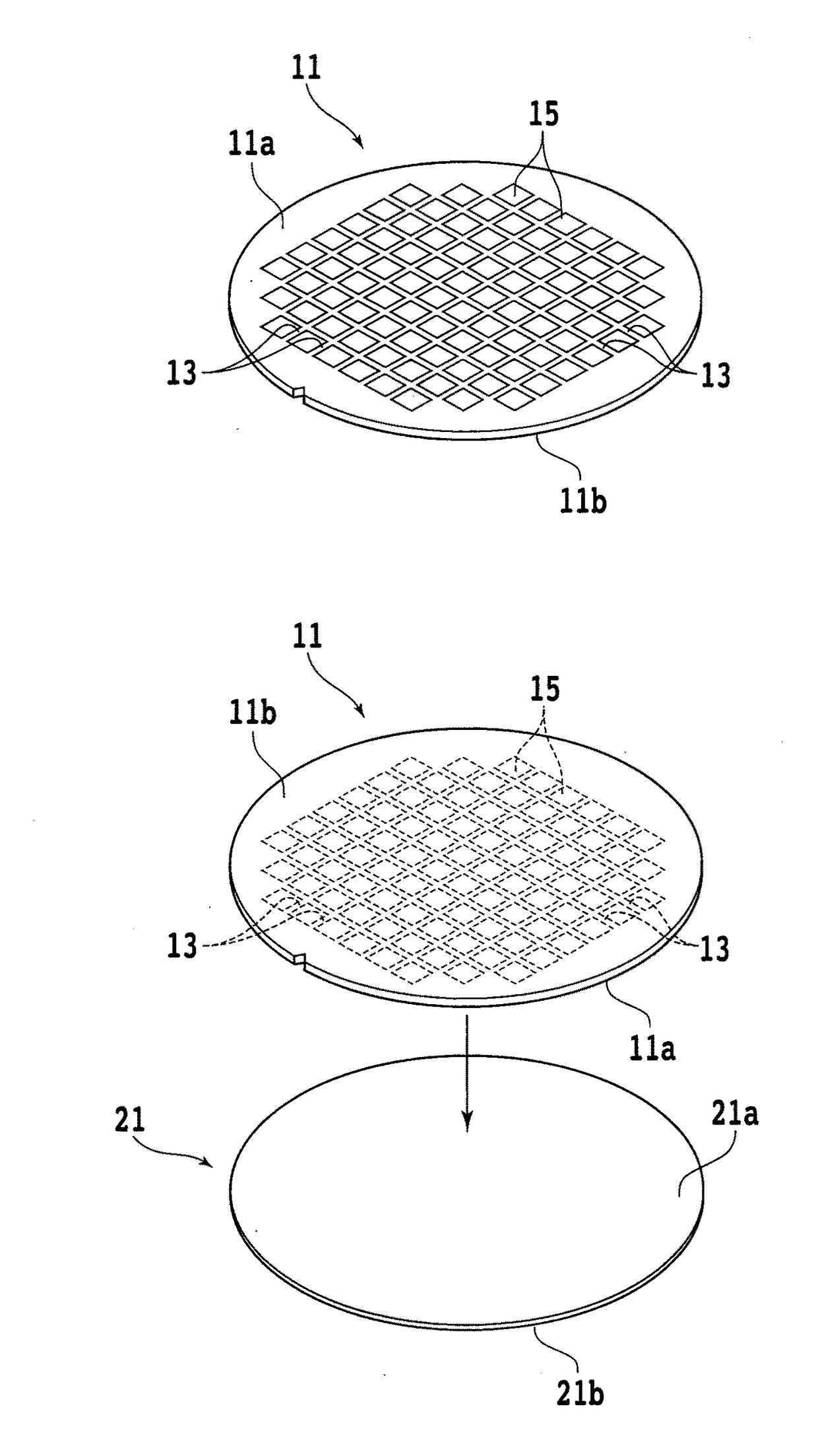
[0019]A method of processing a wafer according to a preferred embodiment of the present invention will be described in detail below with reference to the drawings. The method of processing a wafer according to the present embodiment includes a protective member applying step (see FIG. 1B), a first grinding step (see FIGS. 2A and 2B), and a second grinding step (see FIGS. 3A and 3B). In the protective member applying step, a protective member is applied to the face side of a wafer which has a device area where a plurality of devices are formed and an outer circumferential excess area surrounding the device area. In the first grinding step, the reverse side of the wafer which corresponds to the device area is ground using a grinding wheel that is smaller in diameter than the wafer, forming a thin first portion and a thick second portion surrounding the thin first portion. In the first grinding step, the grinding wheel is moved relatively to the wafer so that the reverse side of the fi...
PUM
 Abstract
Description
Claims
Application Information
 - R&D Engineer
- R&D Manager
- IP Professional
- Industry Leading Data Capabilities
- Powerful AI technology
- Patent DNA Extraction
Browse by: Latest US Patents, China's latest patents, Technical Efficacy Thesaurus, Application Domain, Technology Topic, Popular Technical Reports.
© 2024 PatSnap. All rights reserved.Legal|Privacy policy|Modern Slavery Act Transparency Statement|Sitemap|About US| Contact US: help@patsnap.com