Semiconductor device evaluation jig, semiconductor device evaluation apparatus, and semiconductor device evaluation method

a semiconductor device and evaluation apparatus technology, applied in the direction of individual semiconductor device testing, heat measurement, instruments, etc., can solve the problems of inaccurate measurement of the temperature of the semiconductor device itself, difficulty in measuring temperature, and error in the temperature characteristic itself, so as to achieve the effect of precise detection of temperatur

Active Publication Date: 2018-03-29
MITSUBISHI ELECTRIC CORP
View PDF3 Cites 4 Cited by
  • Summary
  • Abstract
  • Description
  • Claims
  • Application Information

AI Technical Summary

Benefits of technology

[0012]In accordance with the present invention, the through hole is formed in the base, and therefore, the semiconductor device can be secured to and in close contact with the base by vacuum suction from the stage. Accordingly, the temperature of the semiconductor device can be detected by the temperature detecting element through the electrically conductive base, and thus the temperature of the semiconductor device can precisely be detected.
[0013]Moreover, the first electrode pad which is electrically connected to the temperature detecting element is formed in the first surface side. Accordingly, use of the semiconductor device evaluation jig of the present invention enables use of an existing semiconductor device evaluation apparatus and thereby enables precise detection of the temperature of the semiconductor device in the above-described manner. A new semiconductor device evaluation apparatus is thus unnecessary to prepare.

Problems solved by technology

Particularly regarding evaluation of a temperature characteristic, unstable measurement of the temperature of the semiconductor device under evaluation results in an error in the temperature characteristic itself.
This method, however, is accompanied by movement of heat due to the contact and therefore does not accurately measure the temperature of the semiconductor device itself.
However, when the surface of the semiconductor device is a mirror surface, the temperature is difficult to measure.
Therefore, this type of method does not accurately measure the temperature of the semiconductor device.

Method used


Image

  • Semiconductor device evaluation jig, semiconductor device evaluation apparatus, and semiconductor device evaluation method
  • Semiconductor device evaluation jig, semiconductor device evaluation apparatus, and semiconductor device evaluation method
  • Semiconductor device evaluation jig, semiconductor device evaluation apparatus, and semiconductor device evaluation method

Examples


first embodiment

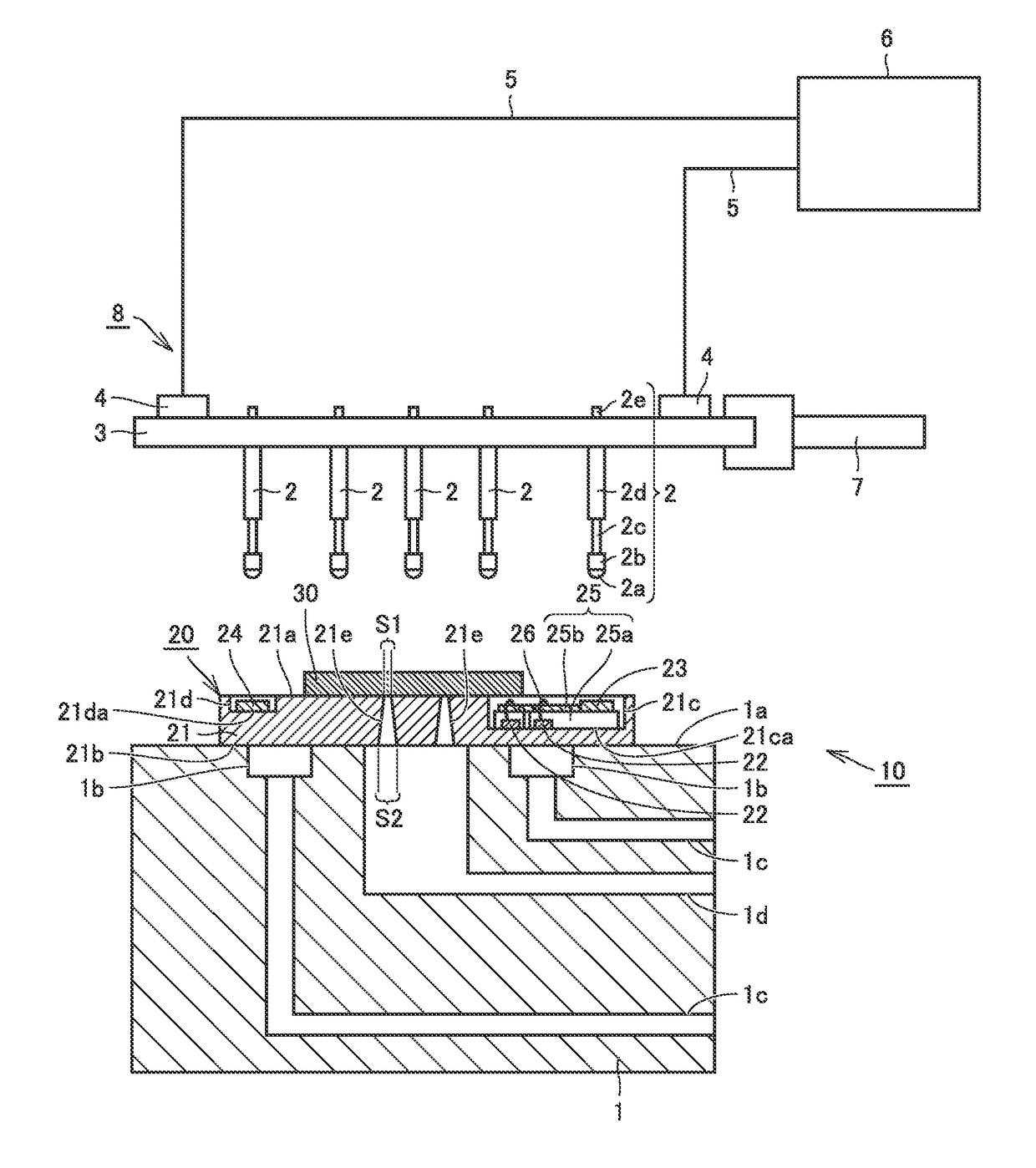
[0027]Initially, a configuration of a semiconductor device evaluation apparatus in the present embodiment will be described with reference to FIG. 1.

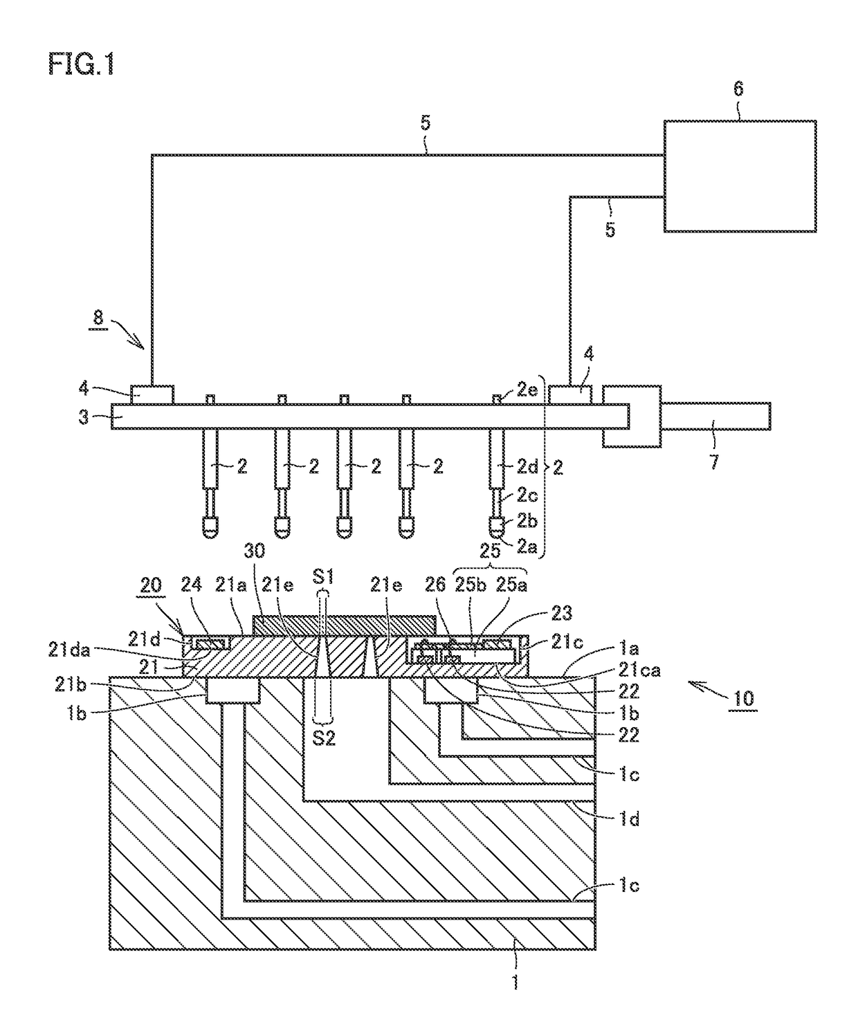
[0028]FIG. 1 is a diagram schematically showing the configuration of the semiconductor device evaluation apparatus in the present embodiment. As shown in FIG. 1, semiconductor device evaluation apparatus 10 mainly includes a chuck stage (stage) 1, a plurality of contact probes (probes) 2, an insulating base (insulating support member) 3, a connecting portion 4, a signal line 5, an evaluation unit (control unit) 6, a moving arm 7, and a semiconductor device evaluation jig 20.

[0029]Chuck stage 1 is a table having a surface 1a, and semiconductor device evaluation jig 20 is set in contact with and secured to surface 1a. Chuck stage 1 is configured to be capable of securing semiconductor device evaluation jig 20 as well as a semiconductor device 30 by vacuum suction.

[0030]Specifically, in chuck stage 1, a suction groove 1b and suction holes ...

second embodiment

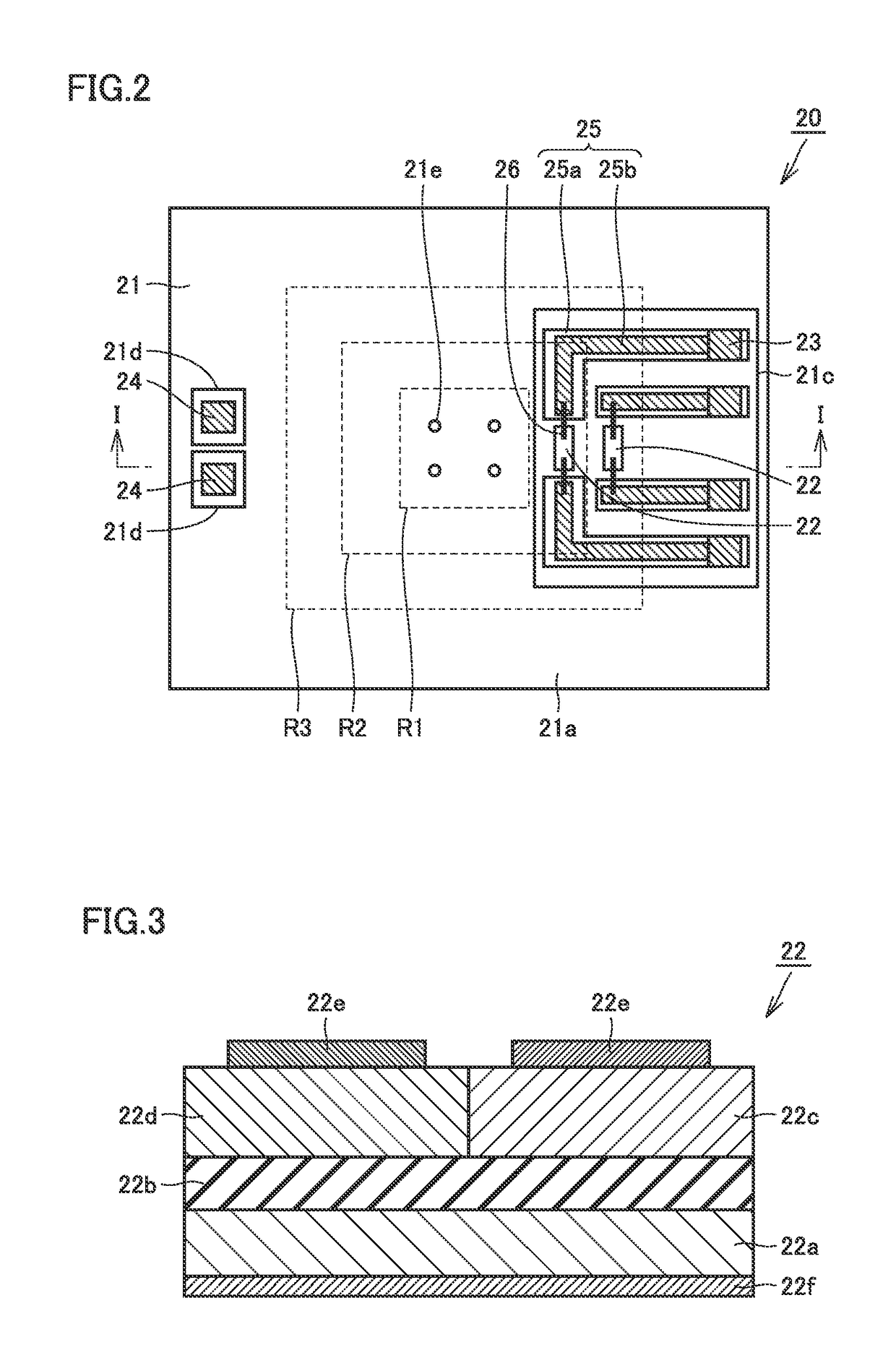
[0116]FIGS. 7 and 8 are respectively a plan view and a rear view schematically showing a configuration of a semiconductor device evaluation jig in the present embodiment. FIG. 9 is a schematic cross-sectional view of the semiconductor device evaluation jig and a semiconductor device along line IX-IX in FIG. 7.

[0117]As shown in FIGS. 7 to 9, the configuration in the present embodiment differs from the configuration in the first embodiment in that temperature detecting element 22, electrode pad 23, interconnecting portion 25, and connection wire 26 are located in the back surface 21b side of base 21 and attached to base 21 in the present embodiment.

[0118]As shown mainly in FIGS. 8 and 9, recess 21c in the present embodiment is formed in back surface 21b of base 21, rather than front surface 21a of base 21. In recess 21c, temperature detecting element 22, interconnecting portion 25, and connection wire 26 are disposed.

[0119]Temperature detecting element 22 is attached to base 21 by die...

third embodiment

[0128]FIG. 10 is a partial cross-sectional view schematically showing a configuration of a semiconductor device evaluation jig and a semiconductor device in the present embodiment. As shown in FIG. 10, the configuration in the present embodiment differs from the configuration in the first embodiment in that a side surface 21cb of recess 21c is inclined and temperature detecting element 22 is attached to the inclined side surface 21cb in the present embodiment.

[0129]Side surface 21cb is inclined with respect to front surface 21a of base 21 and forms an obtuse angle with bottom 21ca of recess 21c. Side surface 21cb formed as an inclined surface is a side surface within mount regions R2, R3 (namely the side surface located directly below semiconductor device 30 when semiconductor device 30 is mounted).

[0130]Features of the present embodiment other than the above-described ones are substantially identical to those of the first embodiment. Therefore, the same elements are denoted by the ...


PUM

PropertyMeasurementUnit
electrical characteristicaaaaaaaaaa
electrical conductivityaaaaaaaaaa
temperatureaaaaaaaaaa

Abstract

A base having electrical conductivity and a plate shape for a semiconductor device evaluation jig has a front surface which includes a mount region where a semiconductor device is to be mounted. In this mount region, the base has a through hole extending through the base. A temperature detecting element is attached to the base. An electrode pad is electrically connected to the temperature detecting element and formed in the front surface side.

Description

TECHNICAL FIELD[0001]The present invention relates to a semiconductor device evaluation jig, a semiconductor device evaluation apparatus, and a semiconductor device evaluation method, and particularly relates to a semiconductor device evaluation jig having a temperature detecting element for detecting the temperature of a semiconductor device, a semiconductor device evaluation apparatus, and a semiconductor device evaluation method.BACKGROUND ART[0002]When the electrical characteristic of a semiconductor device which is an object to be measured is evaluated, it is important to precisely measure the temperature of the semiconductor device under evaluation. Particularly regarding evaluation of a temperature characteristic, unstable measurement of the temperature of the semiconductor device under evaluation results in an error in the temperature characteristic itself. Moreover, when the electrical characteristic is evaluated in order to address the requirement to apply large current / hi...

Claims


Application Information

Patent Timeline
Patent Type & Authority Applications(United States)
IPC IPC(8): G01R31/26G01K7/00
CPCG01R31/2601G01K7/00G01K1/14G01R31/26G01K7/01G01K2007/163G01R1/0408G01R1/0433G01R1/0483
Inventor NOGUCHI, TAKAYAOKADA, AKIRAMOCHIZUKI, KOICHI
Owner MITSUBISHI ELECTRIC CORP
Why Eureka
Try Eureka