Molded resin-sealed power semiconductor device

Active Publication Date: 2018-04-05
MITSUBISHI ELECTRIC CORP
View PDF2 Cites 1 Cited by
  • Summary
  • Abstract
  • Description
  • Claims
  • Application Information

AI Technical Summary

Benefits of technology

The invention is a power semiconductor device that is molded with resin and has increased flexibility in its layout. This allows for the creation of a small and low-cost device.

Problems solved by technology

The semiconductor element and inner lead are reflow soldered to the lead frame, but as mounting is carried out on only one side, considerable deformation occurs due to thermal contraction when the rigidity of the lead frame is low.
As the molded resin (wire holding portion) protrudes beyond the exposed surface of the lead frame, the external wire needs to be isolated by providing a step in the heatsink, and there is a problem in that restrictions occur in the heatsink manufacturing method and layout, and cost cannot be reduced.
Also, the structure of the existing molded resin-sealed power semiconductor device disclosed in Patent Document 1 is such that an allowable current value of the aluminum wire is low, because of which there is a problem in that multiple pieces of wire bonding are needed, and size and cost cannot be reduced.

Method used


Image

  • Molded resin-sealed power semiconductor device
  • Molded resin-sealed power semiconductor device
  • Molded resin-sealed power semiconductor device

Examples


first embodiment

[0016]Hereafter, based on the drawings, a first embodiment of the invention will be described. Identical reference signs in the drawings indicate identical or corresponding portions.

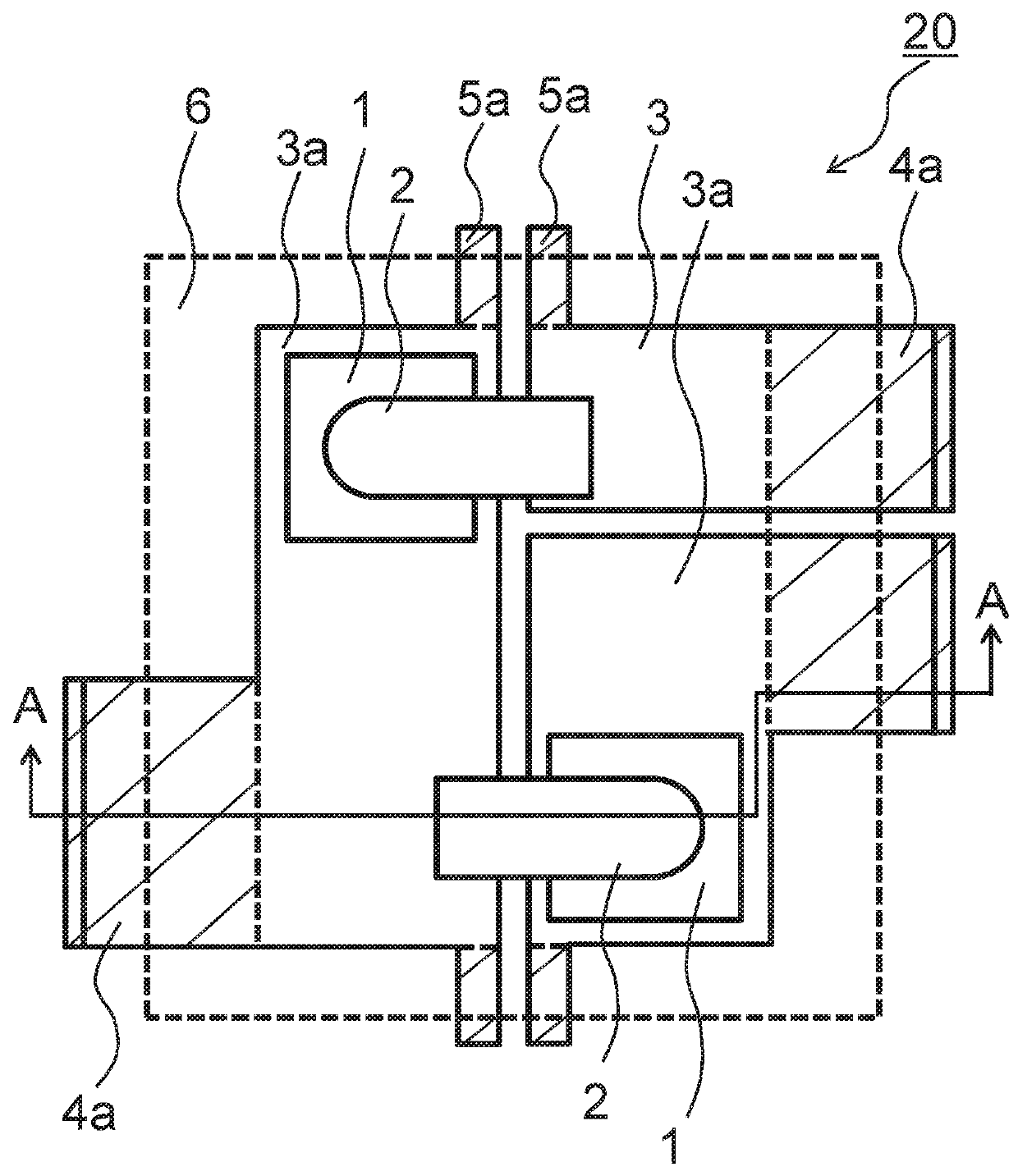
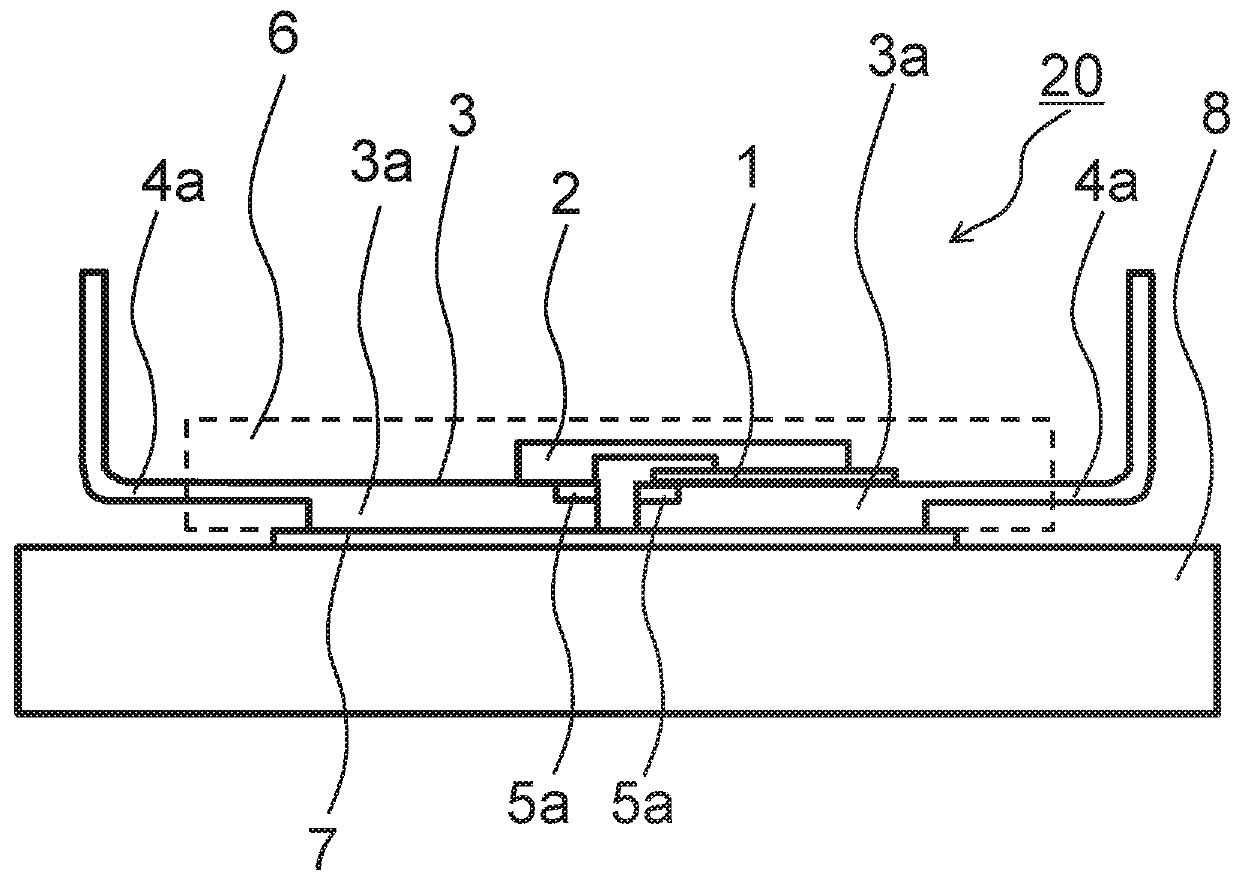
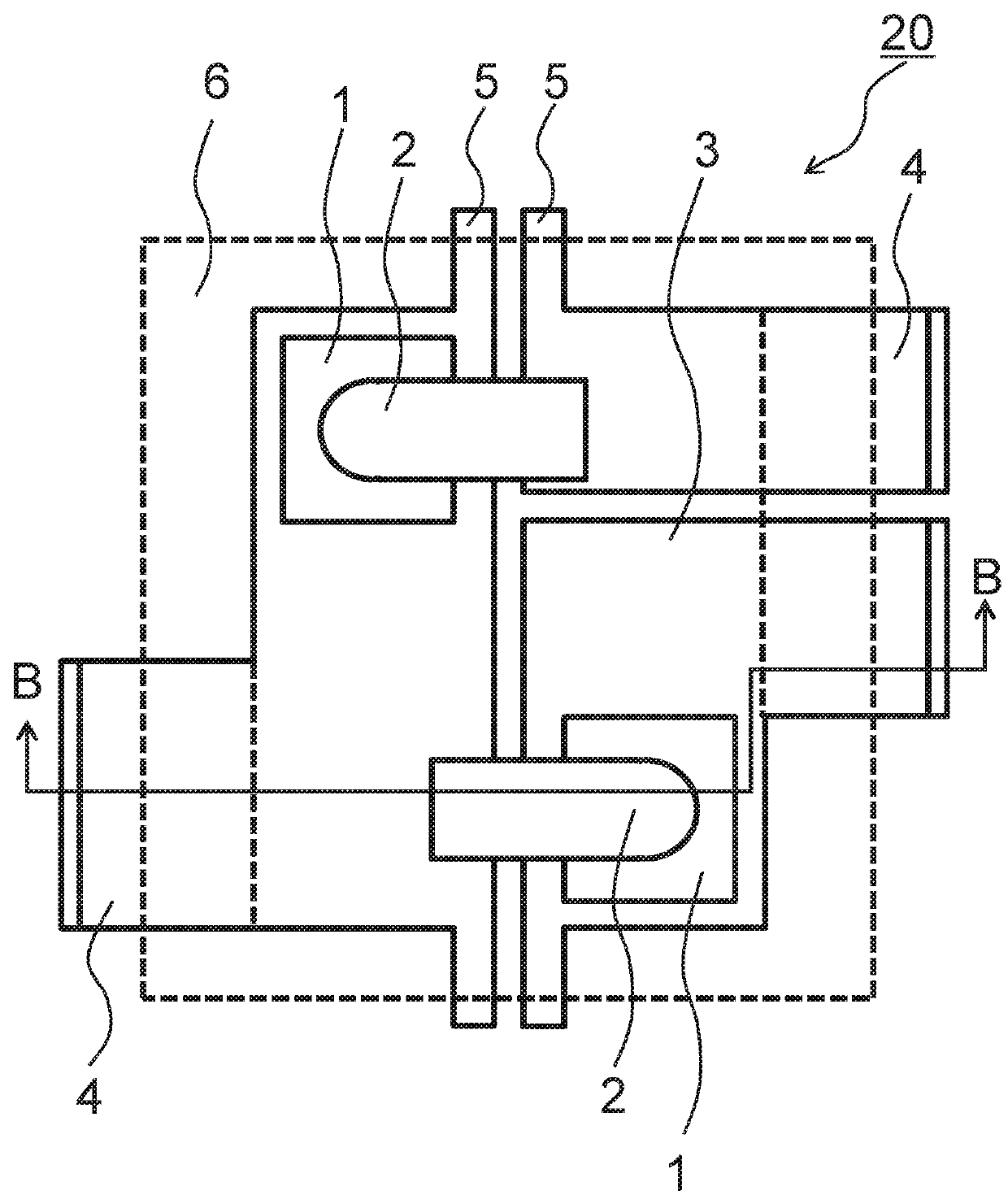
[0017]FIG. 1 is a plan view schematically showing a molded resin-sealed power semiconductor device according to the first embodiment of the invention. Also, FIG. 2 is a sectional view along an A-A line of the power semiconductor device in FIG. 1.

[0018]In FIGS. 1 and 2, a power semiconductor device 20 includes a power semiconductor element 1 that carries out power conversion in accordance with a switching operation, a lead frame 3 in which the power semiconductor element 1 is mounted, an inner lead 2 that electrically connects an electrode (not shown) of the power semiconductor element 1 and an electrode (not shown) of the lead frame 3, and a molded resin 6 formed so as to seal the power semiconductor element 1, inner lead 2, and lead frame 3.

[0019]The lead frame 3, which has differing thicknesses, has a ...


PUM


Abstract

Freedom of layout is increased, and a small, low-priced molded resin-sealed power semiconductor device is obtained. A molded resin-sealed power semiconductor device includes a power semiconductor element, a lead frame having a thick portion on which the power semiconductor element is mounted and a thin portion thinner than the thick portion, an inner lead that electrically connects the power semiconductor element and lead frame, and a molded resin that seals the power semiconductor element, lead frame, and inner lead.

Description

BACKGROUND OF THE INVENTIONField of the Invention[0001]The present invention relates to a molded resin-sealed power semiconductor device formed by, for example, sealing with a molded resin.Description of the Related Art[0002]An existing general molded resin-sealed power semiconductor device is such that a semiconductor element and inner lead are soldered to a lead frame on which a catch portion is provided, and the whole is sealed with a molded resin. Cooling of the semiconductor element is essential, and the lead frame, including an external wire and the catch portion, needs to be isolated from a heatsink, because of which the lead frame is fixed across an insulating sheet to a projecting portion of the heatsink.[0003]The semiconductor element and inner lead are reflow soldered to the lead frame, but as mounting is carried out on only one side, considerable deformation occurs due to thermal contraction when the rigidity of the lead frame is low. As the lead frame is corrected so as...

Claims


Application Information

Patent Timeline
IPC IPC(8): H01L23/367H01L23/31H01L23/495H01L23/29
CPCH01L23/3675H01L23/293H01L23/49548H01L23/3121H01L2924/181H01L2224/40245H01L23/3107H01L23/49524H01L23/49562H01L23/49575H01L2924/00012
Inventor ISHII, RYUICHI
Owner MITSUBISHI ELECTRIC CORP
Why Eureka
Try Eureka