Pixel compensation circuit

a compensation circuit and pixel technology, applied in the direction of instruments, static indicating devices, etc., can solve the problems of unfavorable image properties, voltage drop (ir drop) effect, many drawbacks of conventional technologies, etc., and achieve the effect of improving the brightness uniformity of an active matrix organic ligh

Active Publication Date: 2018-04-19
INT TECH
View PDF0 Cites 1 Cited by
  • Summary
  • Abstract
  • Description
  • Claims
  • Application Information

AI Technical Summary

Benefits of technology

[0010]The present invention relates to a pixel compensation circuit, and particularly, to a pixel compensation circuit for improving brightness uniformity of an active-matrix organic light emitting diode (AMOLED).

Problems solved by technology

When the thin film transistors in different sub-pixels have too much difference in component electrical properties, an uneven image property would be formed.
In addition, another major problem occurring in the current driving system is the voltage drop (IR-drop) effect, which is generated when the distal voltage drop is caused by the electrical load of the system.
Accordingly, the conventional technologies have many drawbacks and need to be improved.

Method used


Image

  • Pixel compensation circuit
  • Pixel compensation circuit
  • Pixel compensation circuit

Examples


Embodiment Construction

[0027]The present invention is described in detail with reference to the accompanying drawings that clearly illustrate objectives, technical solution and advantages of the present invention.

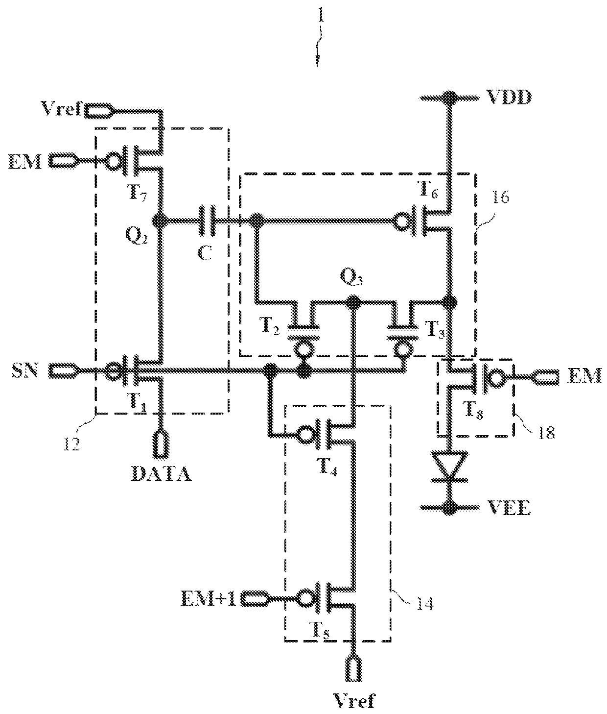
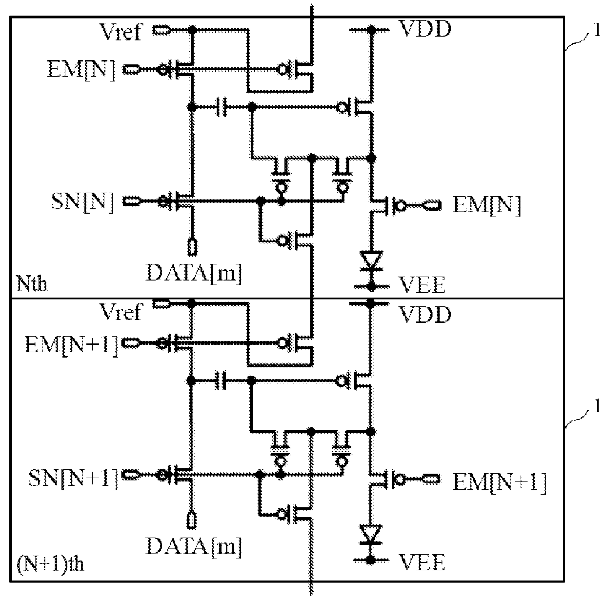
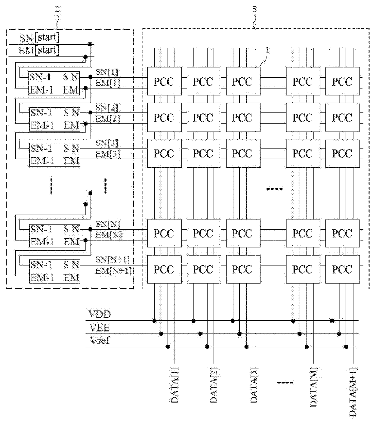
[0028]Please refer to FIG. 1, which is a schematic view showing a pixel compensation circuit according to an embodiment of the present invention. One aspect of the present invention provides a pixel compensation circuit 1. According to one embodiment of the present invention, the pixel compensation circuit 1 includes an input module 12, a reset module 14, a data processing module 16 and a switch module 18. The input module 12 receives a reference level Vref and a data signal DATA, and responds to a light emission control signal EM and a scan signal SN, so as to produce a first signal. The reset module 14 receives the reference level Vref and responds to a sub-light emission control signal EM+1 and the scan signal SN, so as to produce a reset signal. The data processing module 16 receives the firs...


PUM


Abstract

A pixel compensation circuit is arranged for compensating the critical parameter associated with the electrical properties of the components in thin film transistors of an active matrix organic light emitting diode display or similar illumination systems to avoid uneven brightness resulted from the voltage drop effect. The pixel compensation circuit is defined in a sub-pixel area, wherein there are eight thin film transistors and one capacitor, and the circuit is operated by two control signals. In contrast, three control signals are required in the conventional technologies. The fewer control signals are required, which is benefit to the flexibility of the layout and design of specification.

Description

BACKGROUND[0001]Currently, an active matrix organic light emitting diode (AMOLED) display is the focus of the display field due to its amazing image quality and optical specification better than the conventional display.[0002]The AMOLED display is used as an emitter with current through an organic light emitting diode, the current is controlled by an active matrix, and brightness of gray scale is determined by an amount of the current during light emission.[0003]The active matrix is composed of a group of pixel units, and an effective area of light emission is defined by resolution. The effective area of light emission is an area of pixel units multiplied by a resolution in a vertical direction and then multiplied by a resolution in a horizontal direction.[0004]A typical pixel unit is composed of three sub-pixel units. Generally, a sub-pixel unit is composed of a plurality of thin film transistors and capacitors, a gray scale of emission brightness of a sub-pixel area is controlled ...

Claims


Application Information

Patent Timeline
Patent Type & Authority Applications(United States)
IPC IPC(8): G09G3/3233
CPCG09G3/3233G09G2300/0439G09G2300/0404G09G2300/0819G09G2320/0233G09G2300/0426G09G2310/08G09G3/3266G09G3/3275G09G2300/0842G09G2300/0861G09G2310/0262G09G2320/045
Inventor CHENG, SHIH-SONG
Owner INT TECH
Why Eureka
Try Eureka