Flip-flop

a flip-flop and flip-flop technology, applied in the field of flip-flops, can solve the problems that the conventional master-slave flip-flop cannot meet the low power level, and the conventional master-slave flip-flop consumes power, so as to prevent unnecessary power consumption and low power

Active Publication Date: 2018-05-24
SAMSUNG ELECTRONICS CO LTD
View PDF3 Cites 1 Cited by
  • Summary
  • Abstract
  • Description
  • Claims
  • Application Information

AI Technical Summary

Benefits of technology

[0008]Therefore, a flip-flop according to some example embodiments may include an internal node that is charged by inverted input data (e.g., data generated by inverting input data) and an internal node that is charged by the input data, where the internal nodes complementarily operate (e.g., node-values of the internal nodes are complementarily determined) because the internal nodes are cross-connected, so that the flip-flop may prevent unnecessary power consumption while the input data is not changed. That is, the flip-flop may operate with low power by preventing the internal nodes from being repeatedly charged and discharged in response to a clock signal while the input data is not changed.

Problems solved by technology

However, since a conventional master-slave flip-flop includes internal nodes that are repeatedly (e.g., alternately) charged and discharged in response to a clock signal, the conventional master-slave flip-flop consumes power even while input data is not changed.
Thus, the conventional master-slave flip-flop cannot satisfy the low power level that a recent mobile device of which an operating frequency is relatively high requires.

Method used


Image

  • Flip-flop
  • Flip-flop
  • Flip-flop

Examples


Embodiment Construction

[0031]Hereinafter, some example embodiments will be explained in detail with reference to the accompanying drawings.

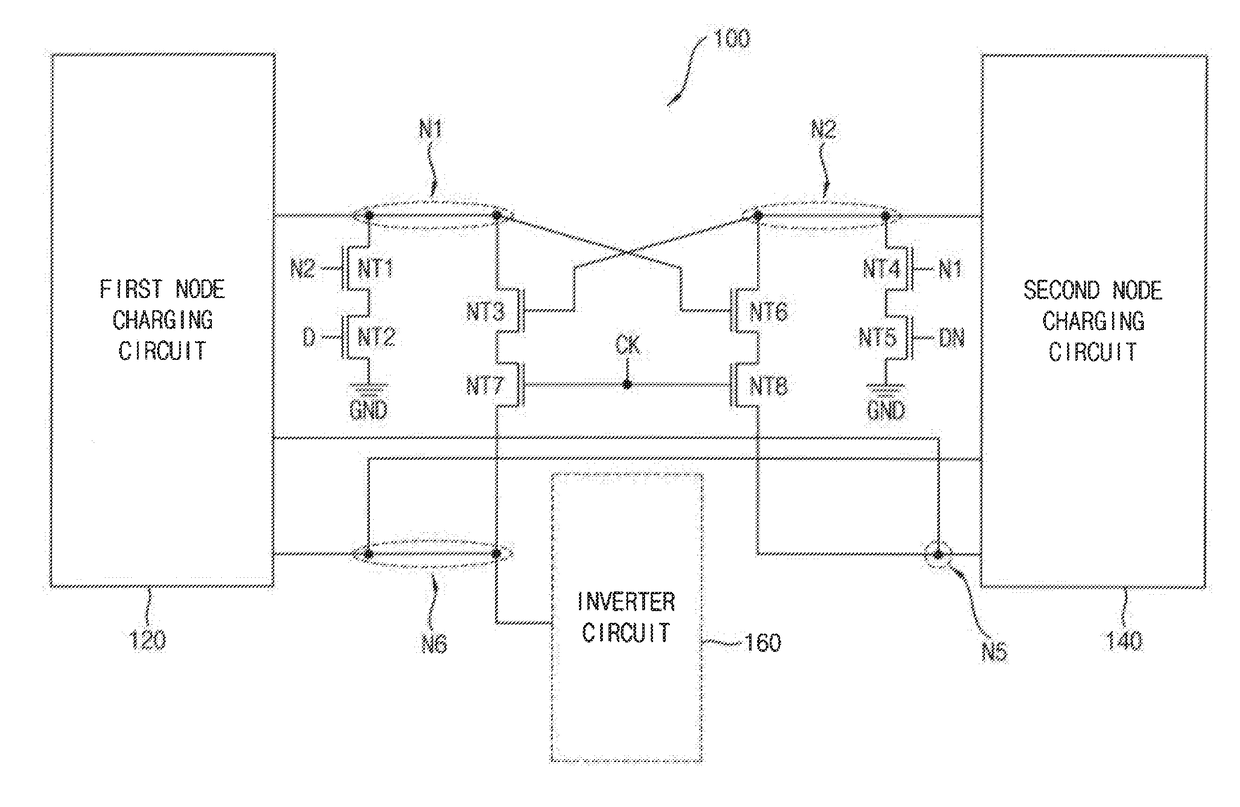
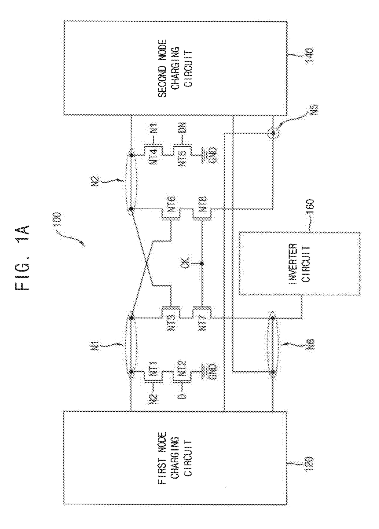
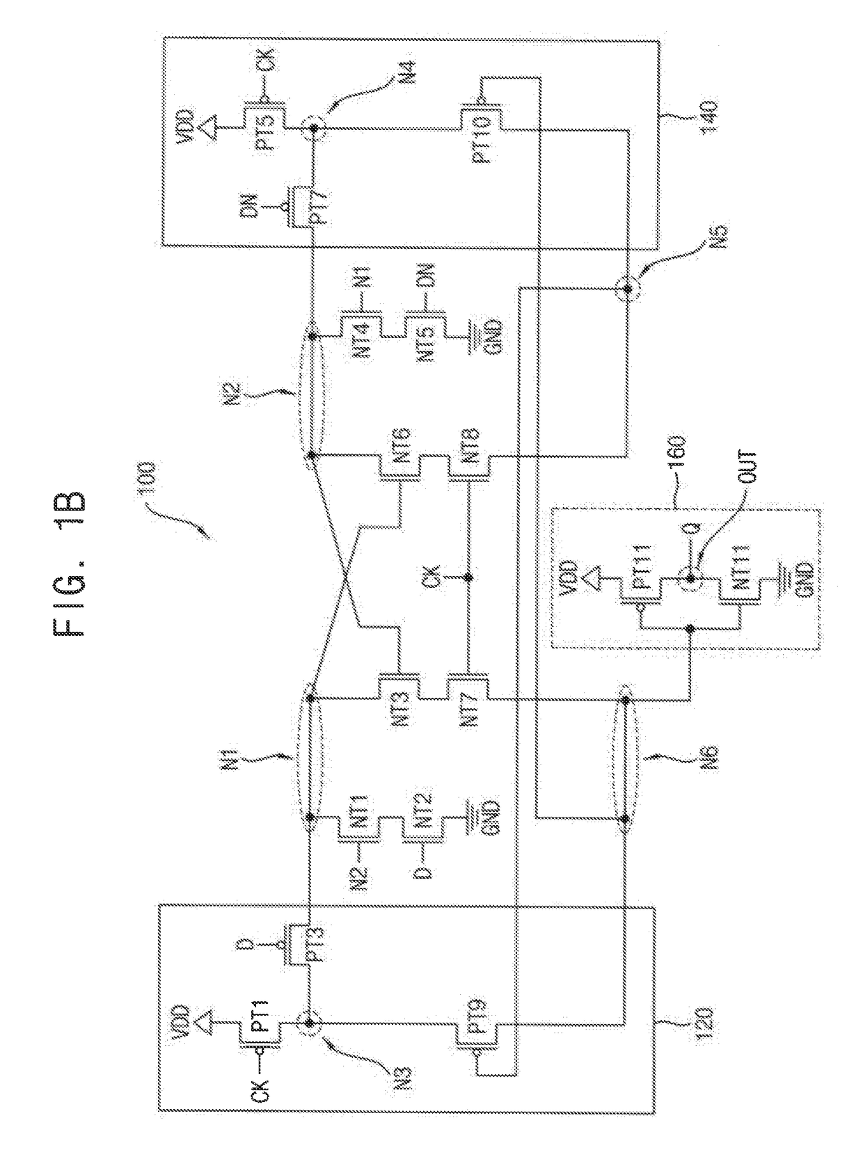
[0032]FIG. 1A is a circuit diagram illustrating a flip-flop according to some example embodiments. FIG. 1B is a detailed circuit diagram illustrating the flip-flop of FIG. 1A. FIG. 2 is a block diagram illustrating an example in which the flip-flop of FIG. 1B is implemented by logic elements. FIG. 3 is a timing diagram illustrating an example in which the flip-flop of FIG. 1B operates.

[0033]Referring to FIGS. 1A through 3, the flip-flop 100 may include a first node charging circuit 120, a second node charging circuit 140, and first through eighth n-channel metal oxide semiconductor (NMOS) transistors NT1 through NT8. In some example embodiments, the flip-flop 100 may further include an inverter circuit 160. Based on the above structure, the flip-flop 100 may latch input data D at rising edges of a clock signal CK and may output latched input data D as output data Q. In...


PUM


Abstract

A flip-flop includes a first node charging circuit configured to charge a first node with inverted input data generated by inverting input data, a second node charging circuit configured to charge a second node with the input data, and first through eighth NMOS transistors. The flip-flop is configured to latch the input data at rising edges of a clock signal and output latched input data as output data. The flip-flop includes an internal circuit configured to charge a sixth node with inverted input data generated by inverting the latched input data.

Description

CROSS-REFERENCE TO RELATED APPLICATION(S)[0001]This application claims priority under 35 USC § 119 to Korean Patent Application No. 10-2016-0156812, filed on Nov. 23, 2016 in the Korean Intellectual Property Office (KIPO), the contents of which are incorporated herein in its entirety by reference.BACKGROUND1. Technical Field[0002]Example embodiments relate generally to a logic circuit. More particularly, some example embodiments relate to a flip-flop that latches input data at rising edges of a clock signal and outputs latched input data as output data.2. Description of the Related Art[0003]Recently, according to a mobile convergence trend, there is a rising interest on a low power technology for a mobile device (e.g., a smart phone, a smart pad, etc.). Generally, since the mobile device uses a limited power such as a battery, manufacturing (or, designing) the mobile device with low power chips including low power flip-flops is necessary as well as efficient power management for the...

Claims


Application Information

Patent Timeline
Patent Type & Authority Applications(United States)
IPC IPC(8): H03K3/012H03K3/356
CPCH03K3/356182H03K3/012H03K3/021H03K19/00346H03K3/35625H03K3/3562H03K3/0372
Inventor HWANG, HYUN-CHULKIM, MIN-SULEE, DAE-SEONG
Owner SAMSUNG ELECTRONICS CO LTD
Why Eureka
Try Eureka