Thin film transistor and display panel using the same

a thin film transistor and display panel technology, applied in the field of thin film transistors and display panels, can solve the problems of increasing the limitation the width of the bezel, and the difficulty of reducing the area occupied by the pixel driving circuit, so as to reduce the area occupied by the transistor, improve the performance of the transistor, and reduce the amount of leakage current

Active Publication Date: 2018-05-31
LG DISPLAY CO LTD
View PDF18 Cites 33 Cited by
  • Summary
  • Abstract
  • Description
  • Claims
  • Application Information

AI Technical Summary

Benefits of technology

[0012]Therefore, the inventors recognized the problems mentioned above and invented a method for reducing the area occupied by the transistor to increase a stability of the driving circuits disposed in the display area or the non-display area and a display panel to which the method is applied.
[0017]A display panel according to an aspect of the present disclosure includes a substrate including a pixel area and a non-pixel area and a dual gate transistor on the non-pixel area. The dual gate transistor includes first and second transistors which are connected in series and an auxiliary electrode which connects two gate electrodes of the first and second transistors. The auxiliary electrode is on a different layer from the gate electrode. Therefore, an area in which the dual gate transistor is formed may be reduced and stability of the driving circuit may be secured.
[0018]A display panel according to an aspect of the present disclosure includes a flexible substrate and a plurality of transistors on the flexible substrate. The plurality of transistors includes a multiple gate transistor in which at least two transistors are connected in series. The multiple gate transistor has a plurality of gate electrodes connected to each other through a contact hole in an insulating layer disposed on the gate electrodes. Therefores, an area in which the multiple gate transistor is formed may be reduced and stability of the driving circuit may be secured.
[0019]A thin film transistor according to another aspect of the present disclosure includes an active layer on a substrate and having two channel layers which are spaced apart from each other, a first insulating layer on the active layer, two gate electrodes which are spaced apart from each other on the first insulating layer to form a dual gate structure, and a source electrode and a drain electrode which are on the active layer with the active layer therebetween and are electrically connected to the active layer through a contact hole on the first insulating layer in which the two gate electrodes are electrically connected to each other through a connection structure disposed on a different layer from the two gate electrodes. Therefore, an area occupied by a thin film transistor having a dual gate structure may be reduced and the stability of the driving circuit may be secured.
[0021]According to the aspects of the present disclosure, at least one of a dual gate transistor, a triple gate transistor, and a multiple gate transistor is disposed in a pixel driving circuit, a data driving circuit, a gate driving circuit, or a touch driving circuit, to reduce the leakage current of the transistor and secure the stability of the device.
[0025]And, according to the aspect of the present disclosure, a plurality of transistors is formed by a polycrystalline silicon active layer with a top-gate structure, so that a performance of the transistor is improved. Further, a gate short-circuit structure is applied, to reduce an amount of the leakage current.

Problems solved by technology

Therefore, in order to implement the stable pixel driving circuit, the pixel driving circuit becomes complicated and an area occupied by the pixel driving circuit is increased.
When the driving circuits which inevitably occupy a predetermined physical space are disposed on the substrate, if the number of transistors is increased to improve stability of the driving circuits, a design method of disposing the transistors according to the related art has limitations in reducing the area occupied by the pixel driving circuit and reducing a width of the bezel.

Method used


Image

  • Thin film transistor and display panel using the same
  • Thin film transistor and display panel using the same
  • Thin film transistor and display panel using the same

Examples


Embodiment Construction

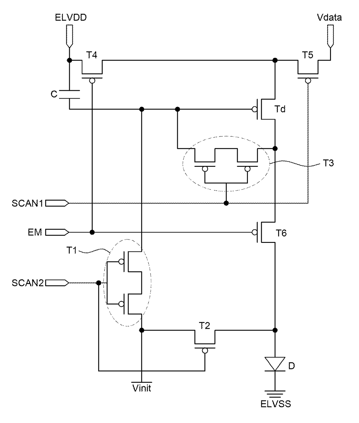
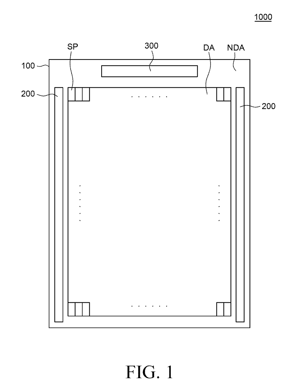
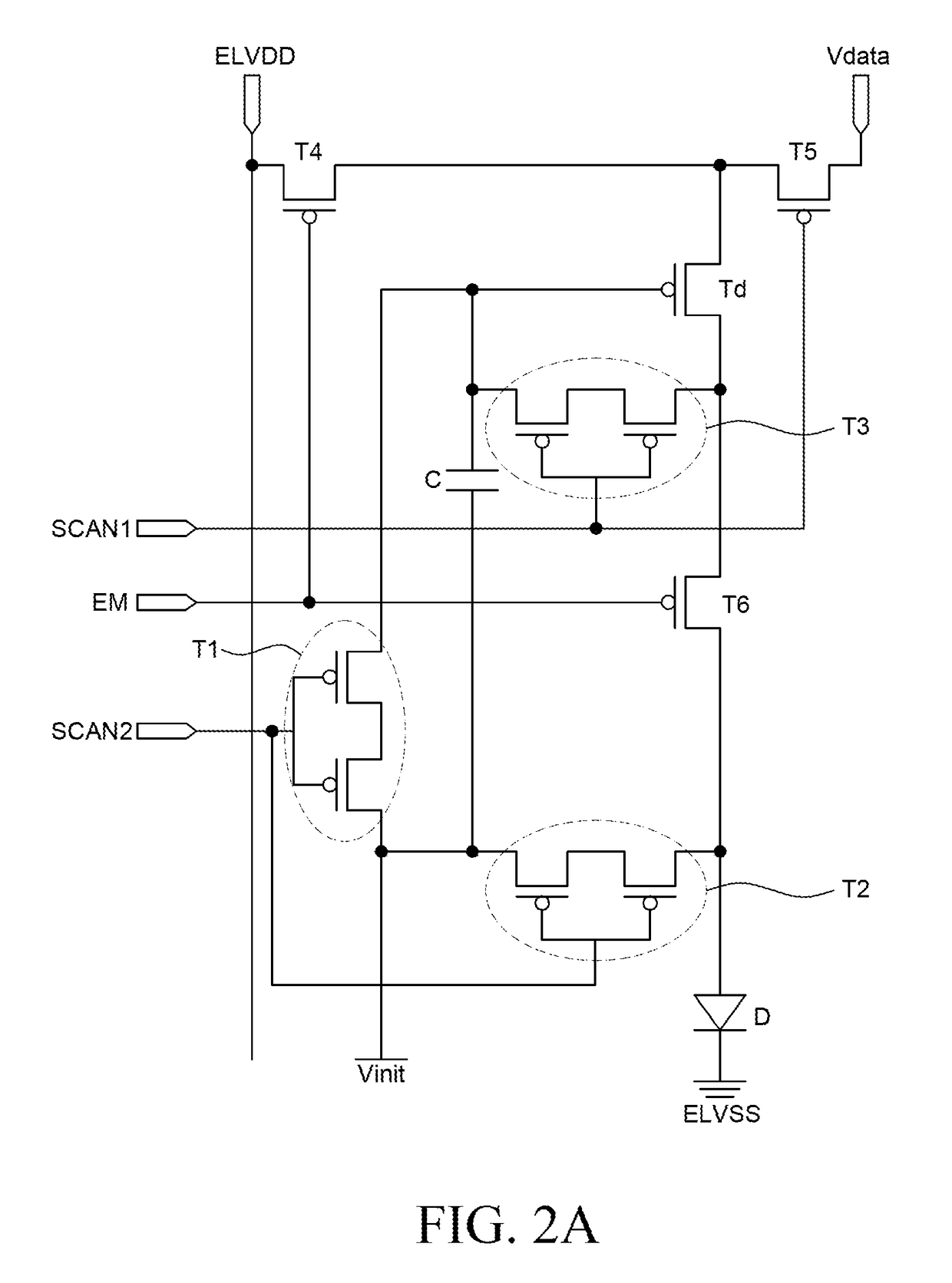
[0044]Advantages and characteristics of the present disclosure and a method of achieving the advantages and characteristics will be clear by referring to aspects described below in detail together with the accompanying drawings. However, the present disclosure is not limited to aspect disclosed herein but will be implemented in various forms. The aspects are provided by way of example only so that a person of ordinary skilled in the art can fully understand the disclosures of the present disclosure and the scope of the present disclosure. Therefore, the present disclosure will be defined only by the scope of the appended claims.

[0045]The shapes, sizes, ratios, angles, numbers, and the like illustrated in the accompanying drawings for describing the aspects of the present disclosure are merely examples, and the present disclosure is not limited thereto. Like reference numerals generally denote like elements throughout the specification. And, in the following description of the presen...


PUM


Abstract

Provided is a display panel to which a dual gate transistor is applied. The display panel includes a substrate including a pixel area and a non-pixel area and a dual gate transistor disposed on the non-pixel area. The dual gate transistor includes first and second transistors which are connected in series and an auxiliary electrode which connects two gate electrodes of the first and second transistors. The auxiliary electrode is on a layer which is different from the gate electrode. Therefore, an area in which the dual gate transistor is formed is reduced and stability of the driving circuit is secured.

Description

CROSS-REFERENCE TO RELATED APPLICATION[0001]This application claims the priority of Korean Patent Application No. 10-2016-0161502 filed on Nov. 30, 2016, in the Korean Intellectual Property Office, the disclosure of which is incorporated herein by reference in its entirety.BACKGROUNDField of the Disclosure[0002]The present disclosure related to a display device and more particularly, to a thin film transistor and a display panel using the same and more in detail, to a thin film transistor having a dual gate structure for implementing a high resolution and a narrow bezel.Description of the Background[0003]As it enters the information era, a display device field which visually displays an electrical information signal is rapidly developing. The display device is used to watch, enjoy, and share not only simple images, but also various contents such as texts, pictures, and videos. Therefore, studies for increasing a resolution of a display device have been continuing to implement a scre...

Claims


Application Information

Patent Timeline
Patent Type & Authority Applications(United States)
IPC IPC(8): H01L27/32G09G3/3291G09G3/3233G09G3/36
CPCH01L27/3248G09G3/3291G09G3/3233H01L27/3262H01L27/3279G09G3/3685H01L2227/323H01L27/1214H01L27/124H01L29/78645G09G2300/0819G09G2300/0842G09G2300/0861G09G2320/0214G09G2320/0238H01L21/823437H01L29/42384H01L29/78696H10K59/1213H10K59/1315H10K59/123H10K59/86H10K59/1201H10K77/111H10K2102/311
Inventor HA, JONGMOO
Owner LG DISPLAY CO LTD
Why Eureka
Try Eureka