Eureka AIR delivers breakthrough ideas for toughest innovation challenges, trusted by R&D personnel around the world.

Method and Apparatus for carrier profiling of semiconductors utilizing simultaneous techniques utilizing a simulator and a Field-Programmable Gate Array

Inactive Publication Date: 2018-06-21
HAGMANN MARK J
View PDF2 Cites 0 Cited by
  • Summary
  • Abstract
  • Description
  • Claims
  • Application Information

AI Technical Summary

Benefits of technology

The invention provides a unified method and apparatus for multiple individual characterization methods. This apparatus is efficient in its ability to run multiple characterization methods and to optionally utilize simulations for real-time analysis of measurements acquired from the multiple carrier profile characterization methods. The invention is also the methodology required to run multiple discrete characterization methods simultaneously. The apparatus comprises necessary components for various methods of carrier profiling being operably connected to a reconfigurable Field-Programmable Gate Array (FPGA) in which a plurality of characterization methodologies and a plurality of simulations can be stored. These features make the invention adaptable to various carrier profiling methodologies and simulations as they become known or discovered. The invention has practical applications in research and development of carrier profiling technologies.

Problems solved by technology

However, none of the previous art describes the use of two or more techniques that are integrated with a simulator in a single instrument.

Method used


Image

  • Method and Apparatus for carrier profiling of semiconductors utilizing simultaneous techniques utilizing a simulator and a Field-Programmable Gate Array
  • Method and Apparatus for carrier profiling of semiconductors utilizing simultaneous techniques utilizing a simulator and a Field-Programmable Gate Array

Examples


Embodiment Construction

[0019]With reference now to the drawings, the preferred embodiment of the apparatus and method is herein described. It should be noted that the articles “a”, “an”, and “the”, as used in this specification, include plural referents unless the content clearly dictates otherwise.

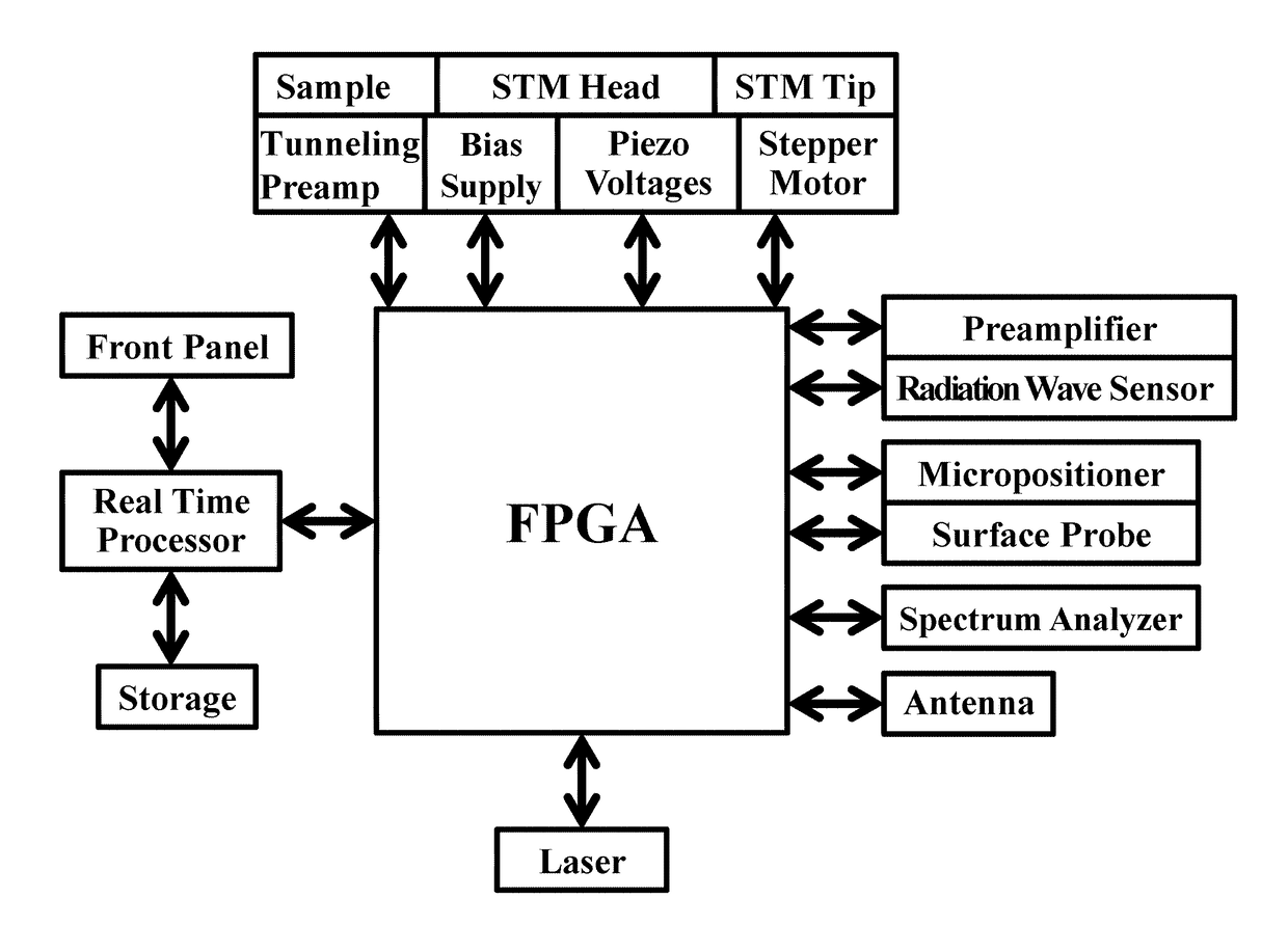
[0020]Referring to the FIGURE, a single instrument performs carrier profiling by any or all of the four techniques which were just described as well as enabling scanning tunneling microscopy in the constant current or constant height mode and scanning tunneling spectroscopy. Furthermore, the instrument provides simulations that may be integrated with the measurements to permit optimization in preparations for a measurement as well as continuous real-time interpretation of the data and automatic adjustments of the parameters in real time as the measurements are made.

[0021]These features are made possible by using a multi-function instrument for which the block diagram is shown in the FIGURE. Note that no persona...


PUM


Abstract

Numerous carrier profiling techniques may be combined for simultaneous operation of those techniques on a single material sample. A single apparatus utilizing a Field-Programmable Gate Array (“FPGA”) may be utilized to simultaneously operate those techniques. Various hardware components necessary for the given techniques may be operationally connected to the FPGA while simulations may be performed and stored with the apparatus for real-time analysis of results.

Description

CROSS-REFERENCES TO RELATED APPLICATIONS[0001]The Application claims priority on prior files U.S. Provisional Application number 62 / 436,265, filed Dec. 19, 2017, and incorporates the same by reference herein in its entirety.FIELD OF THE INVENTION[0002]The present invention relates to the field of carrier profiling of materials and more particularly relates to a method by which a plurality of non-destructive carrier profiling methods is employed on a given sample with the same equipment and optional simulators.BACKGROUND OF THE INVENTION[0003]Others have determined the carrier density of semiconductors by iterating measurements of the tunneling current in a scanning tunneling microscope (STM) with the values of the current which are predicted by accurate three-dimensional simulations on a separate computer [K. Fukuda, M. Nishizawa, T. Tada, L. Boltov, K. Suzuki, S. Satoh, H. Arimoto and T. Kanayama, “Three-dimensional simulation of scanning tunneling microscopy for semiconductor carr...

Claims


Application Information

Patent Timeline
IPC IPC(8): G01Q60/16G01Q10/04
CPCG01Q60/16G01Q10/04G01Q30/04
Inventor HAGMANN, MARK J.
Owner HAGMANN MARK J
Why Eureka
Eureka Blog
Learn More