Substrate, electronic device and display device having the same

a technology of electronic devices and substrates, applied in the direction of electrical apparatus casings/cabinets/drawers, sustainable manufacturing/processing, casings with display/control units, etc., can solve the problems of short-circuit failure between the connection terminals, open-circuit failure between the electronic devices, short-circuit failure between neighboring bumps, etc., to reduce the likelihood or degree of such failures

Active Publication Date: 2018-06-21
SAMSUNG DISPLAY CO LTD
View PDF2 Cites 10 Cited by
  • Summary
  • Abstract
  • Description
  • Claims
  • Application Information

AI Technical Summary

Benefits of technology

[0005]Aspects of example embodiments of the present disclosure relate to a substrate capable of preventing a short-circuit failure or an open-circuit failure caused by conductive particles of an anisotropic conductive film (or capable of reducing a likelihood or degree of such failures), an electronic device, and a display device having the same.

Problems solved by technology

However, when the electronic devices are connected using the ACF, a short-circuit failure may occur between the connection terminals or an open-circuit failure may occur between the electronic devices.
For example, conductive particles included in the ACF may be concentrated around side surfaces of neighboring connection terminals, such as bumps, and a short-circuit failure may occur between the neighboring bumps.
An open-circuit failure may occur between the electronic devices since the conductive particles in the ACF do not contact the bumps having a fine size.

Method used


Image

  • Substrate, electronic device and display device having the same
  • Substrate, electronic device and display device having the same
  • Substrate, electronic device and display device having the same

Examples


Embodiment Construction

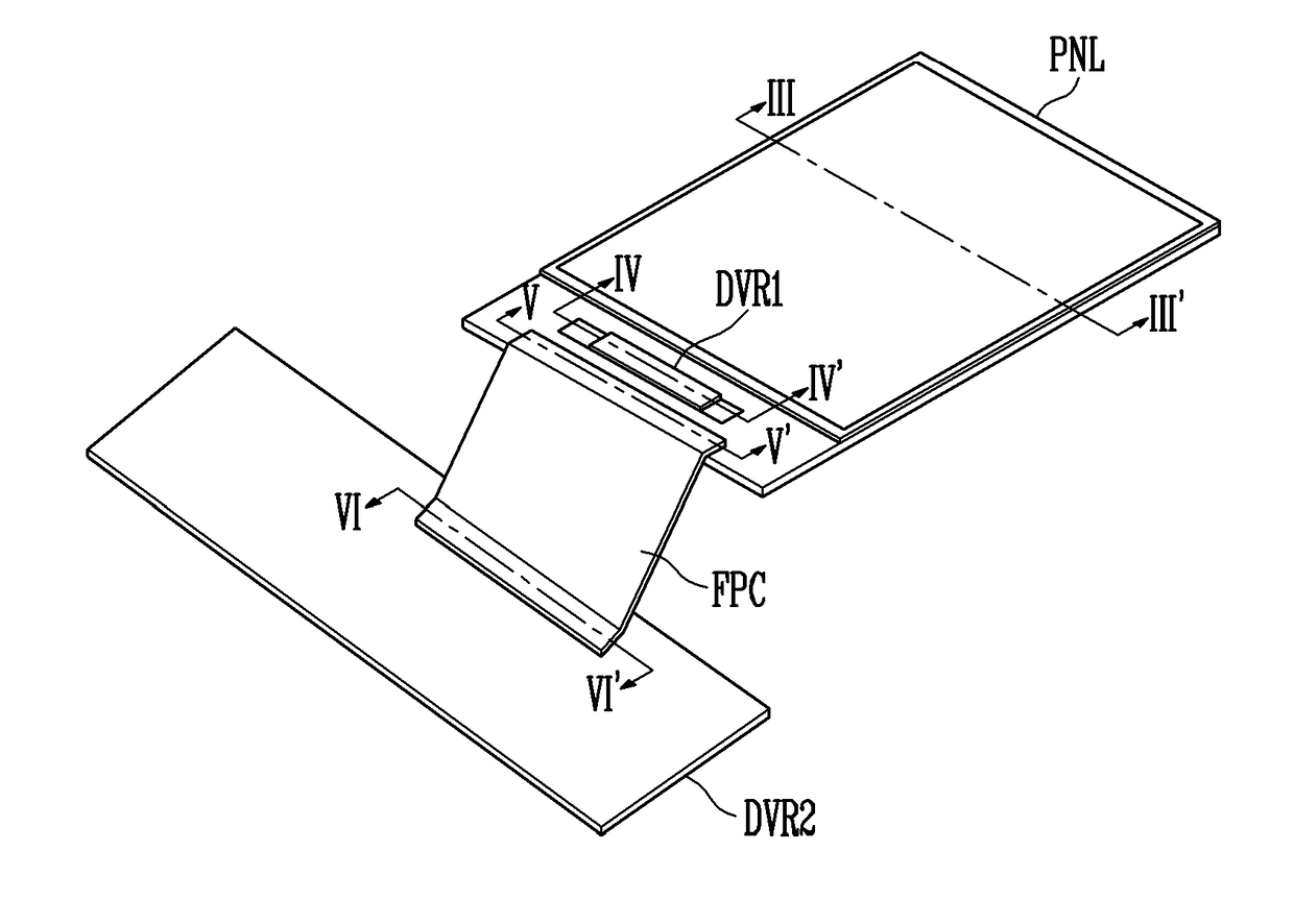
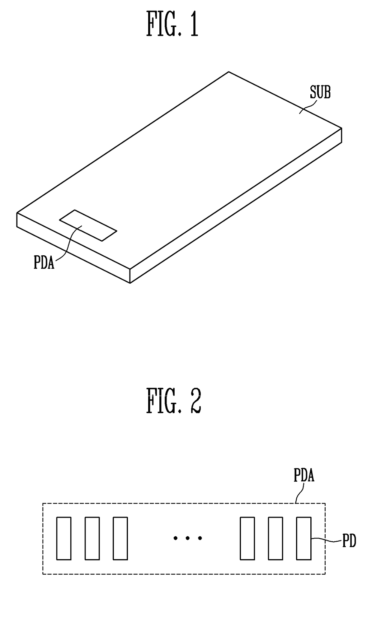
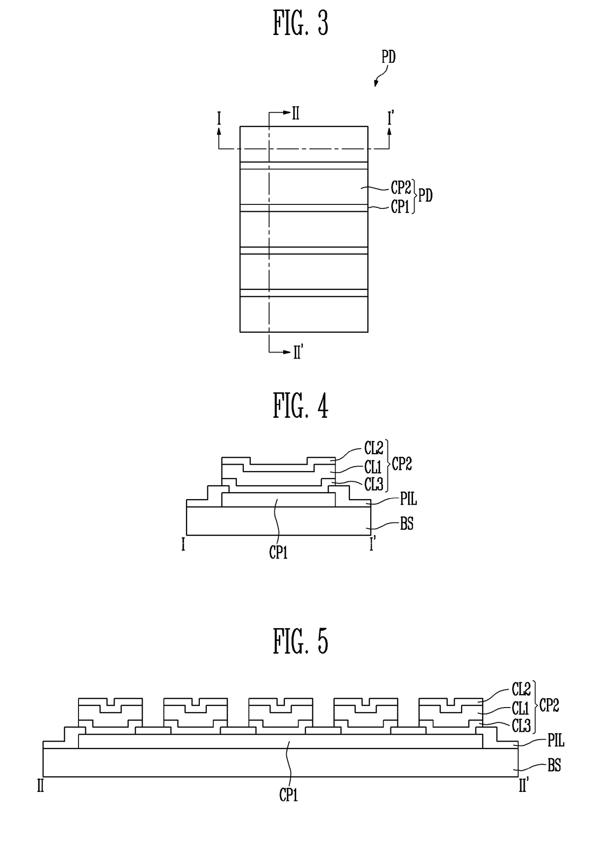
[0043]While aspects of some example embodiments of the present disclosure are described with reference to the accompanying drawings, it is to be understood that various changes and modifications may be made in the present disclosure without departing from the spirit and scope thereof. Further, it should be understood that the present disclosure is not limited to the embodiments disclosed herein, and various changes, equivalences and substitutions may be made without departing from the scope and spirit of the present disclosure.

[0044]Like reference numerals designate like elements throughout the drawings. In the drawings, the dimension of elements may be exaggerated for the clarity of this disclosure. Although terms “first”, “second”, etc. are used herein to describe various elements, these elements should not be limited by these terms. These terms are only used to distinguish one element from another element. For example, the first element may be designated as the second element wit...


PUM


Abstract

A substrate includes a base substrate, and a pad at one side of the base substrate, wherein the pad comprises: a first conductive pattern on the base substrate, an insulating layer including a plurality of contact holes exposing a portion of the first conductive pattern, and second conductive patterns separately on the insulating layer and connected to the first conductive pattern through the plurality of contact holes, wherein side surfaces of the second conductive patterns are exposed.

Description

CROSS-REFERENCE TO RELATED APPLICATION[0001]This application claims priority to and the benefit of Korean Patent Application No. 10-2016-0172753, filed on Dec. 16, 2016, in the Korean Intellectual Property Office, the entire content of which is incorporated herein by reference.BACKGROUND1. Field[0002]Aspects of example embodiments of the present disclosure relate to a substrate, an electronic device, and a display device having the same.2. Description of the Related Art[0003]Recently, high performance and high integration of electronic devices, such as semiconductor devices and display panels, have resulted in a significant increase in number of connection terminals provided in these electronic devices. Therefore, the connection terminals are being reduced in size, and the distance between neighboring connection terminals is also being reduced.[0004]An electronic device may be electrically connected to another electronic device by using an adhesive such as an anisotropic conductive ...

Claims


Application Information

Patent Timeline
Patent Type & Authority Applications(United States)
IPC IPC(8): H01L23/498H01L23/00H05K1/02H05K5/00
CPCH01L23/49811H01L23/49866H01L24/16H05K1/028H05K5/0017H01L2224/16227H01L2224/13144H01L2224/13124H01L2224/13147H01L2224/13111H01L2224/1318H01L27/3246H01L51/5256H01L23/49838H01L24/13H05K1/111H05K3/244H05K2201/0338H05K2203/0285H01L23/4985H01L2224/16106H01L2224/16238H01L2224/81191H01L2224/81815H01L2224/73204H01L2224/32225H01L2224/83104H01L2224/81206H01L24/81H01L2224/05147H01L2224/05139H01L2224/05144H01L2224/05169H01L2224/05164H01L2224/05155H01L2224/05111H01L2224/05124H01L2224/05157H01L2224/05173H01L2224/05178H01L2224/0516H01L2224/05176H01L2224/05163H01L2224/0518H01L2224/05184H01L2224/05179H01L2224/05181H01L2224/05166H01L2224/05113H01L2224/0512H01L2224/05116H01L2224/0519H01L2224/05186H01L2224/05666H01L2224/0568H01L2224/05611H01L2224/05655H01L2224/05686H01L2224/2919H01L2224/0529H01L2224/053Y02P70/50H01L2224/05541H10K59/123H10K59/131H01L2924/00014H01L2224/16225H01L2924/00H01L2924/067H01L2924/0544H01L2924/0105H01L2924/053H01L2924/01049H01L2924/0103H01L2924/0542H01L2924/01051H01L2924/01076H01L2924/06H01L2924/206H01L27/124H05K3/323H01L2924/12044H10K59/129H10K50/80H10K50/8445H10K59/122
Inventor KIM, BYOUNG YONGLEE, JONG HYUKHWANG, JEONG HO
Owner SAMSUNG DISPLAY CO LTD
Why Eureka
Try Eureka