Array substrates and the manufacturing methods thereof, and liquid crystal panels

Inactive Publication Date: 2018-07-05
WUHAN CHINA STAR OPTOELECTRONICS TECH CO LTD
View PDF3 Cites 9 Cited by
  • Summary
  • Abstract
  • Description
  • Claims
  • Application Information

AI Technical Summary

Benefits of technology

The patent text describes a method for manufacturing array substrates by arranging gate lines and touch signal lines on a transparent substrate, and configuring a dielectric layer to cover them. The dielectric layer is then partially removed to create a first through hole, and a touch electrode is added to connect to the touch signal line through the first through hole. The technical effect is to create a structure that allows for efficient and precise placement of touch signal lines and gate lines on a transparent substrate, improving the overall manufacturing process.

Problems solved by technology

If a phone does not have touch capability, it cannot be called as a cellular phone.

Method used


Image

  • Array substrates and the manufacturing methods thereof, and liquid crystal panels
  • Array substrates and the manufacturing methods thereof, and liquid crystal panels
  • Array substrates and the manufacturing methods thereof, and liquid crystal panels

Examples


first embodiment

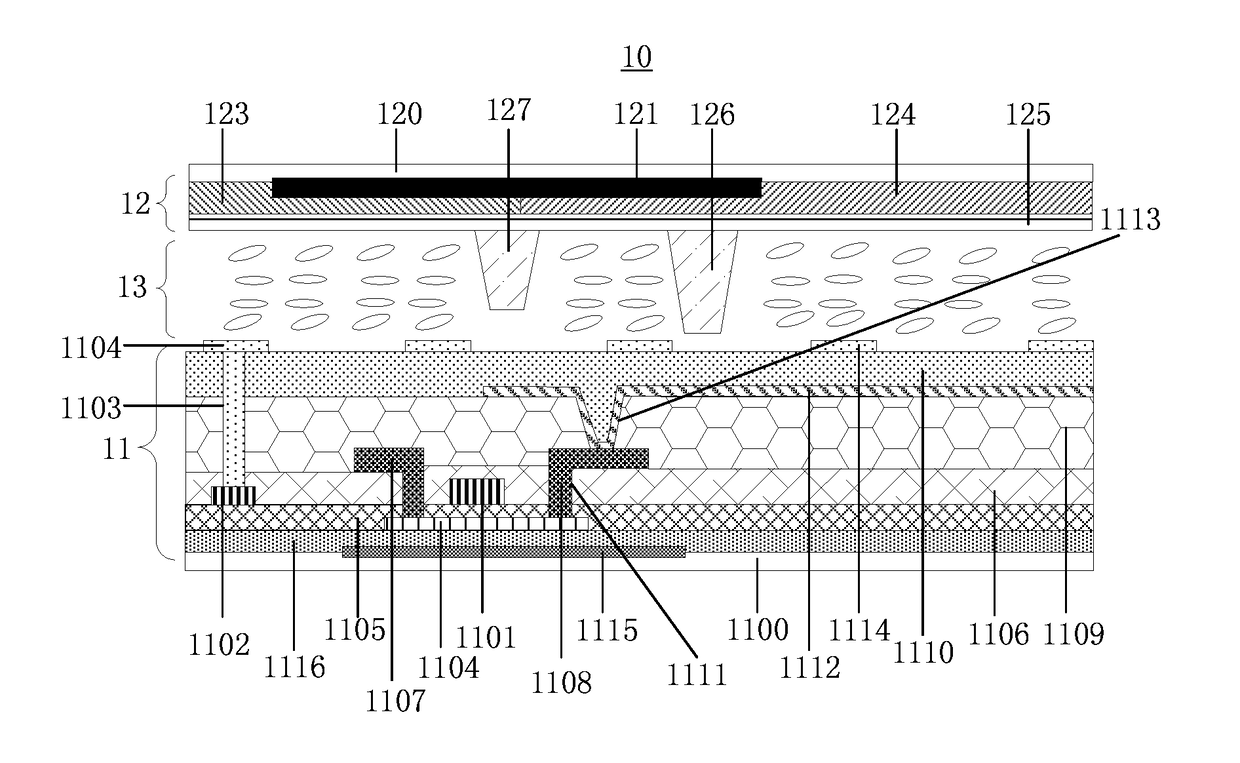
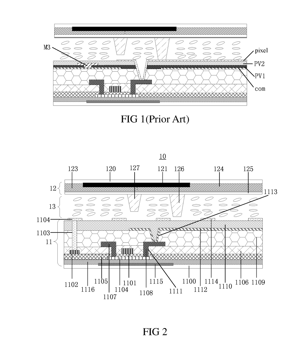
[0028]FIG. 2 is a schematic view of the liquid crystal panel in accordance with a As shown in FIG. 2, the liquid crystal panel 10 includes an array substrate 11, a color-filter (CF) substrate 12, and a liquid crystal layer 13 between the CF substrate 12 and the array substrate 11. The CF substrate 12 includes a glass substrate 120, at least one black matrix 121 on the glass substrate 120, and a filter film, including a red filter film 123, a green filter film 124, and a blue filter film 125. The CF substrate 12 is configured with a post-shaped spacer, including a main post spacer (PS) 126 and a sub post spacer (PS) 127. The post spacers are configured to avoid optical leakage and to operate as a support.

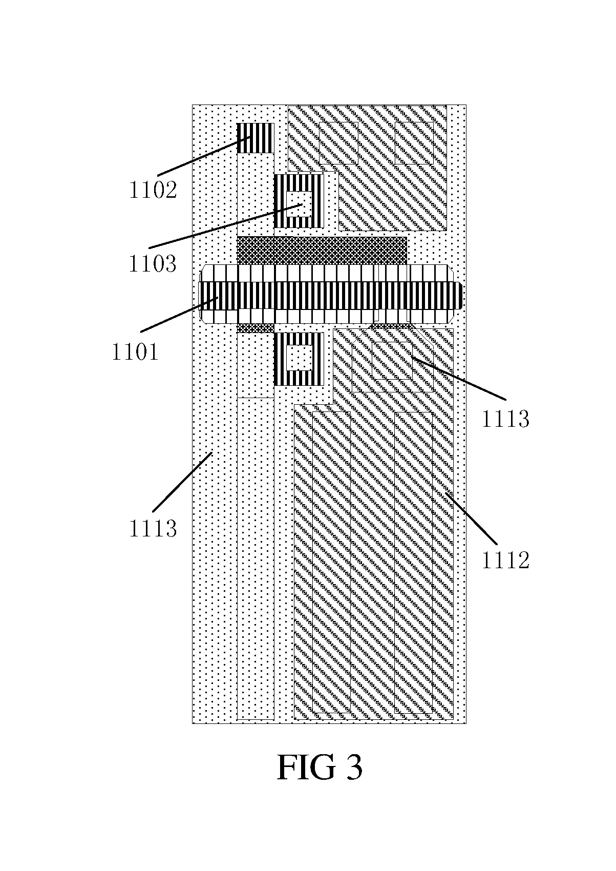
[0029]Referring to FIGS. 2 and 3, the array substrate 11 includes a transparent substrate 1100, a gate line 1101 on the transparent substrate 1100, a touch signal line 1102 on the same layer with the gate line 1101, and a dielectric layer covering the gate line 1101 and the touch si...

second embodiment

[0033]FIG. 4 is a schematic view of the liquid crystal panel in accordance with a The liquid crystal panel 20 includes an array substrate 21, a CF substrate 22, and a liquid crystal layer 23 between the CF substrate 22 and the array substrate 21. The structure of the CF substrate 22 is similar to that in FIG. 2, and thus the descriptions are omitted hereinafter.

[0034]The structure of the array substrate 21 may be referenced in FIGS. 4 and 5. The array substrate 21 includes a transparent substrate 2100, a gate line 2101 on the transparent substrate 2100, a touch electrode line 2102 on the same layer with the gate line 2101, a dielectric layer covering the gate line 2101 and the touch electrode line 2102. In addition, the dielectric layer is configured with a first through hole 2103. The array substrate 21 also includes a touch electrode 2104 arranged on the dielectric layer, and the dielectric layer electrically connects to the touch electrode line 2102 via the first through hole 21...


PUM


Abstract

The present disclosure relates to an array substrate and the manufacturing method thereof, and a liquid crystal panel. The array substrate includes a transparent substrate; a gate line on the transparent substrate; a touch signal line on the same layer with the gate line, and the touch signal line is arranged on the transparent substrate; a dielectric layer covering the gate line and the touch signal line, and the dielectric layer is configured with at least one first through hole; and a touch electrode arranged on the dielectric layer, the touch electrode electrically connects to the touch signal line via the first through hole. In this way, the storage capacitance may be increased, and the pixels may be fully charged when the resolution rate is high. At the same time, the coupling capacitance between the touch electrode and the Rx signal line may be reduced.

Description

BACKGROUND OF THE INVENTION1. Field of the Invention[0001]The present disclosure relates to liquid crystal display technology, and more particularly to an array substrate and the manufacturing method thereof, and a liquid crystal panel.2. Discussion of the Related Art[0002]Touch has been a main function of cellular phones. If a phone does not have touch capability, it cannot be called as a cellular phone. Touch technology may include one glass solution (OGS). The touch panel may be embedded between the color filter substrate and a polarizer, i.e., on cell, and may be embedded into the liquid crystal pixels, i.e., in cell. Currently, with respect to the in cell Touch, the common electrode (Com) within the AA area is divided into small blocks, which operate as touch electrodes. Each of the touch electrodes includes a Rx signal line connecting to the Pin of the output end of the IC. Under the circumstance, a metal layer has to be configured to operate as the Rx signal line to transmit ...

Claims


Application Information

Patent Timeline
IPC IPC(8): G02F1/1333G02F1/1339G02F1/1343G02F1/1362G02F1/1368G06F3/041
CPCG02F1/13338G02F1/13394G02F1/134363G02F1/136286G02F1/1368G02F1/13439G02F1/133345G06F3/0412G02F1/136209G02F2001/13606G02F2001/13685G02F2001/136295G02F2001/13396G02F1/136227G02F2001/136231G02F1/134309G02F1/134372G02F1/13396G02F1/13606G02F1/13685G02F1/136231G02F1/136295
Inventor PENG, XIANGYICHEN, GUILI, YAFENG
Owner WUHAN CHINA STAR OPTOELECTRONICS TECH CO LTD
Why Eureka
Try Eureka