Eureka AIR delivers breakthrough ideas for toughest innovation challenges, trusted by R&D personnel around the world.

Package structure of optical module

Inactive Publication Date: 2018-07-05
LINGSEN PRECISION INDS
View PDF6 Cites 0 Cited by
  • Summary
  • Abstract
  • Description
  • Claims
  • Application Information

AI Technical Summary

Benefits of technology

The present invention provides a package structure for optical modules that reduces the stress placed on the chips, improving their efficiency and stability. This is achieved by using die attach films during the molding process, which alleviates the impact of molding on the chips. Overall, this package structure enhances the performance and efficiency of the optical module.

Problems solved by technology

In the two times of molding of the aforesaid manufacturing process, the stress applied on the light-emitting chip and the sensing chip may affect the properties of the chips, lowering the stability of the chips or even making the chips lose efficiency.
Therefore, the conventional optical sensing module still has drawbacks and needs improvements.

Method used


Image

  • Package structure of optical module
  • Package structure of optical module

Examples


Embodiment Construction

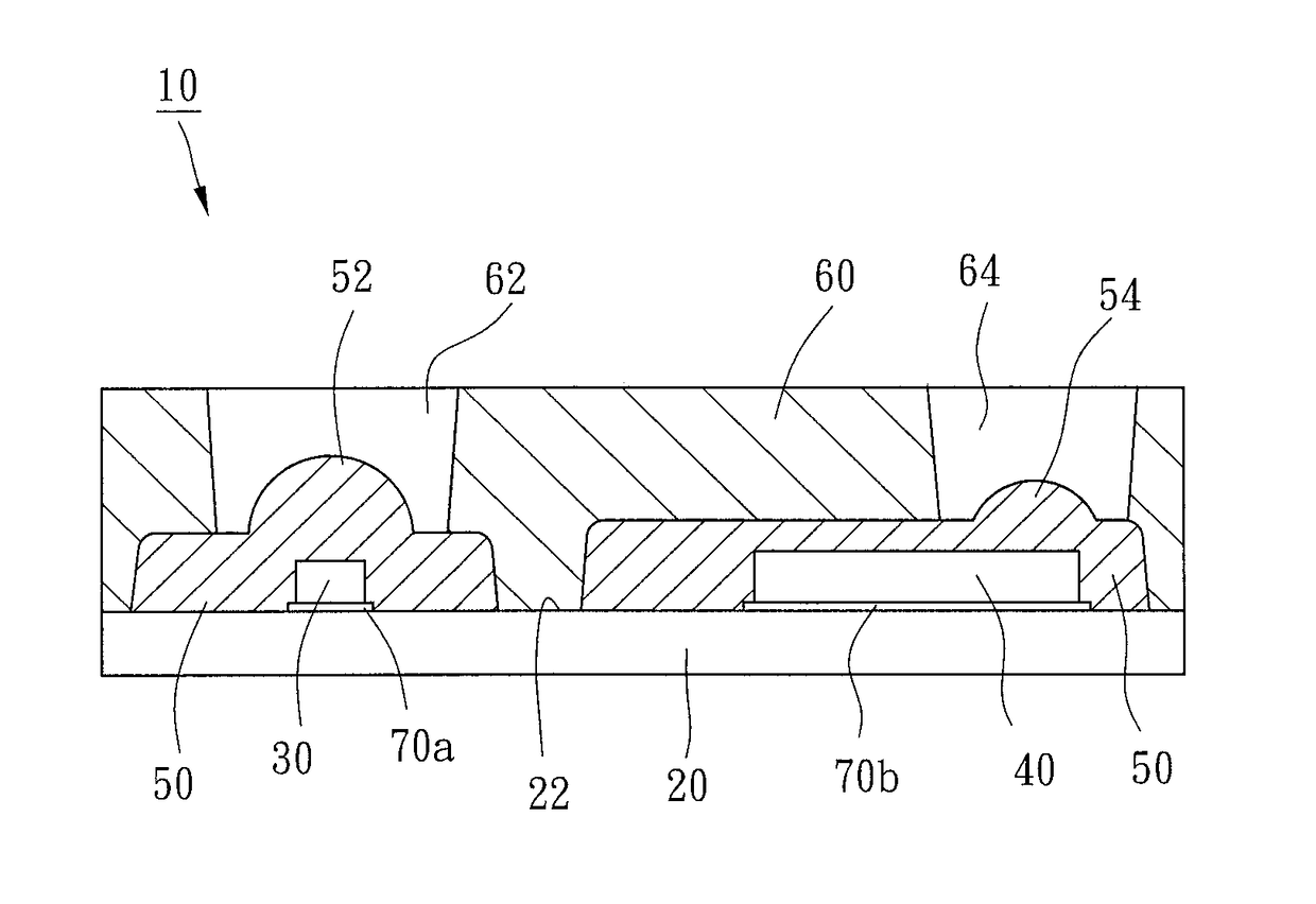
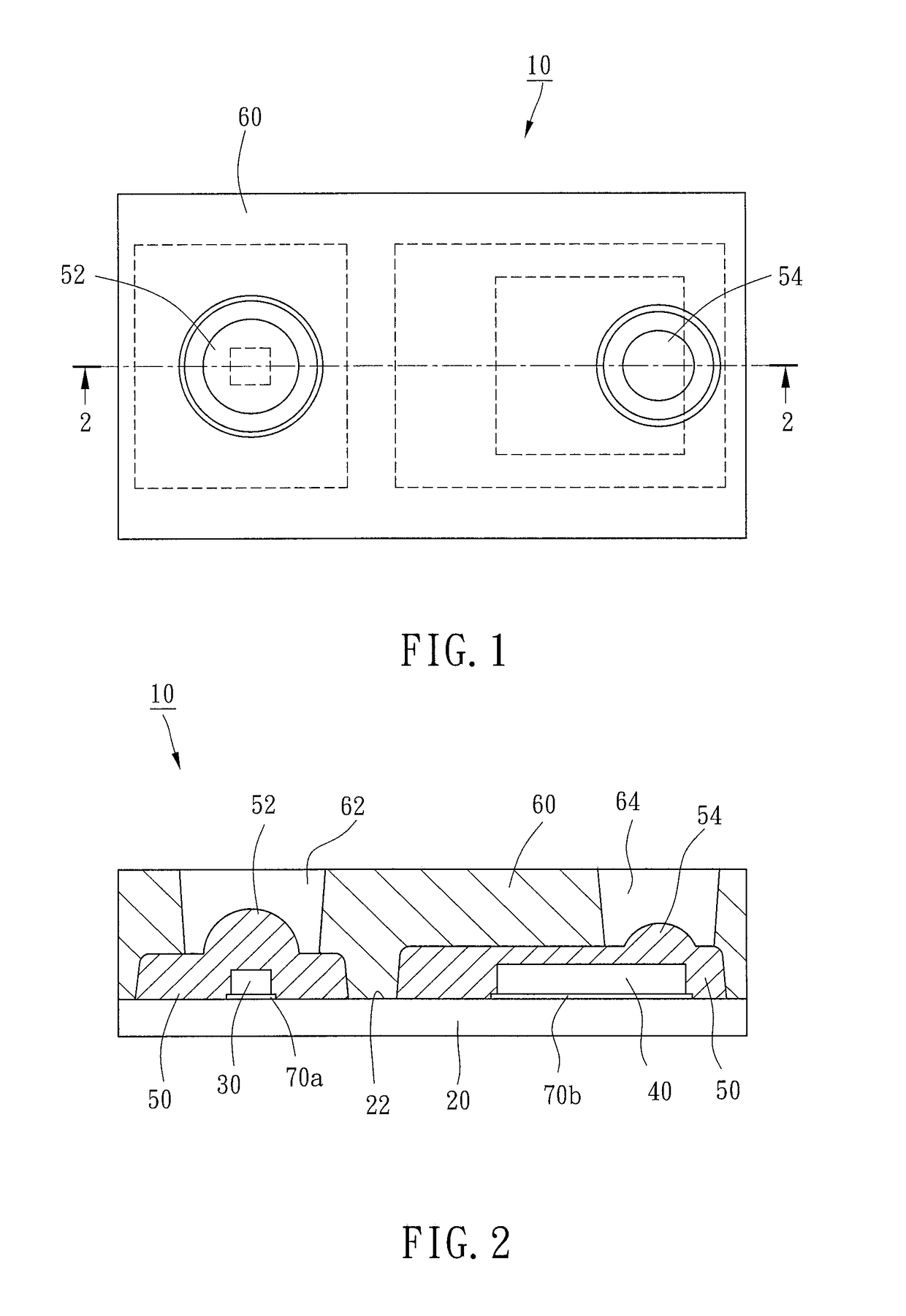
[0012]Referring to FIGS. 1-2, a package structure 10 of an optical module according to a preferred embodiment of the present invention includes a substrate 20, a light-emitting chip 30, a sensing chip 40, two packaging gel bodies 50, and a cover layer 60.

[0013]The substrate 20 in this preferred embodiment may, but unlimited to, be a bismaleimide-triazine (usually referred to as “BT”) substrate, a glass fiber substrate (usually referred to as “FR4”), or a direct bonded copper (usually referred to as “DBC”) substrate. In this way, the manufacturing cost of the substrate 20 is relatively lower. The substrate 20 has a bearing surface 22.

[0014]The light-emitting chip 30 is disposed on the bearing surface 22 by a die attach film 70a. In this preferred embodiment, the light-emitting chip 30 is an LED chip for emitting a light source.

[0015]The sensing chip 40 is disposed on the bearing surface 22 by a die attach film 70b and separated from the light-emitting chip 30. The sensing chip 40 is ...


PUM


Abstract

A package structure of an optical module includes a substrate, a light-emitting chip, a sensing chip, two packaging gel bodies, and a cover layer. The substrate has a bearing surface. The light-emitting chip is disposed on the bearing surface by a die attach film. The sensing chip is disposed on the bearing surface by another die attach film and separated from the light-emitting chip. The two packaging gel bodies cover the light-emitting chip and the sensing chip respectively. The cover layer is disposed on the bearing surface and the two packaging gel bodies and provided with a light-emitting hole located above the light-emitting chip and a light-receiving hole located above the sensing chip.

Description

BACKGROUND OF THE INVENTION1. Field of the Invention[0001]The present invention relates generally to package structures and more particularly, to a package structure of an optical module.2. Description of the Related Art[0002]The optical sensing module is applied very widely, such as in automatic machines and intelligent devices. An example of that is the smart phone. When the smart phone is taken close to the cheek of the user or put into the pocket, the optical sensing module disposed in the smart phone will shut down the screen of the phone for saving electricity or preventing the user from accidentally touching the screen. The theory is that the optical sensing module can emit a light source by a light-emitting chip, such as an LED chip; after being reflected by an exterior object, the light source can be received by a sensing chip of the optical sensing module and transformed into electronic signal for the subsequent processing.[0003]The conventional optical sensing module is m...

Claims


Application Information

Patent Timeline
IPC IPC(8): H01L25/16H01L31/0232H01L31/16
CPCH01L25/167H01L31/16H01L31/02327H01L31/0203G01S7/4811G01S7/4813G01S17/04
Inventor TU, MING-TELIN, CHING-ILEE, CHIH-WEI
Owner LINGSEN PRECISION INDS
Why Eureka
Eureka Blog
Learn More