Imaging devices for use with additive manufacturing systems and methods of monitoring and inspecting additive manufacturing components

a technology of additive manufacturing and imaging devices, applied in the field of additive manufacturing systems, can solve the problems of reducing the quality of layers and components, generating undesirable features, and causing heat variation

Active Publication Date: 2018-07-12
GENERAL ELECTRIC CO
View PDF0 Cites 7 Cited by
  • Summary
  • Abstract
  • Description
  • Claims
  • Application Information

AI Technical Summary

Problems solved by technology

In some known additive manufacturing systems, layer and component quality is reduced due to variation in heat being transferred to the metal powder by the focused laser within the melt pool.
In addition, in some known additive manufacturing systems, heat variation also induces porosity within the build layers.
Moreover, variation in laser position is also known to generate these undesirable features within the additively manufactured component.
However, the imaging devices generate images of only visible portions of the component and thus do not capture subsurface features.
However, ultrasound imaging requires that the component be finished, thus further expending time and materials costs for a potentially undesirable part.
Additionally, x-ray imaging is typically performed by a digital x-ray or Computer Tomography (CT) scans which are limited by the size of the component and also requires a large amount of x-ray energy to penetrate the entire component.
However, not all features, for example, cracking features, are correctable by HIP.

Method used


Image

  • Imaging devices for use with additive manufacturing systems and methods of monitoring and inspecting additive manufacturing components
  • Imaging devices for use with additive manufacturing systems and methods of monitoring and inspecting additive manufacturing components
  • Imaging devices for use with additive manufacturing systems and methods of monitoring and inspecting additive manufacturing components

Examples


Embodiment Construction

[0021]In the following specification and the claims, reference will be made to a number of terms, which shall be defined to have the following meanings.

[0022]The singular forms “a”, “an”, and “the” include plural references unless the context clearly dictates otherwise.

[0023]“Optional” or “optionally” means that the subsequently described event or circumstance may or may not occur, and that the description includes instances where the event occurs and instances where it does not.

[0024]Approximating language, as used herein throughout the specification and claims, may be applied to modify any quantitative representation that could permissibly vary without resulting in a change in the basic function to which it is related. Accordingly, a value modified by a term or terms, such as “about”, “approximately”, and “substantially”, are not to be limited to the precise value specified. In at least some instances, the approximating language may correspond to the precision of an instrument for...


PUM

PropertyMeasurementUnit
mean particle sizeaaaaaaaaaa
depthaaaaaaaaaa

Abstract

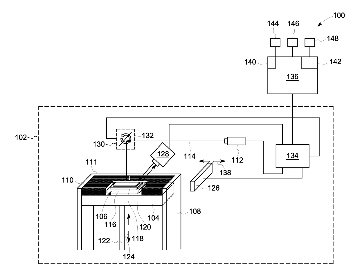
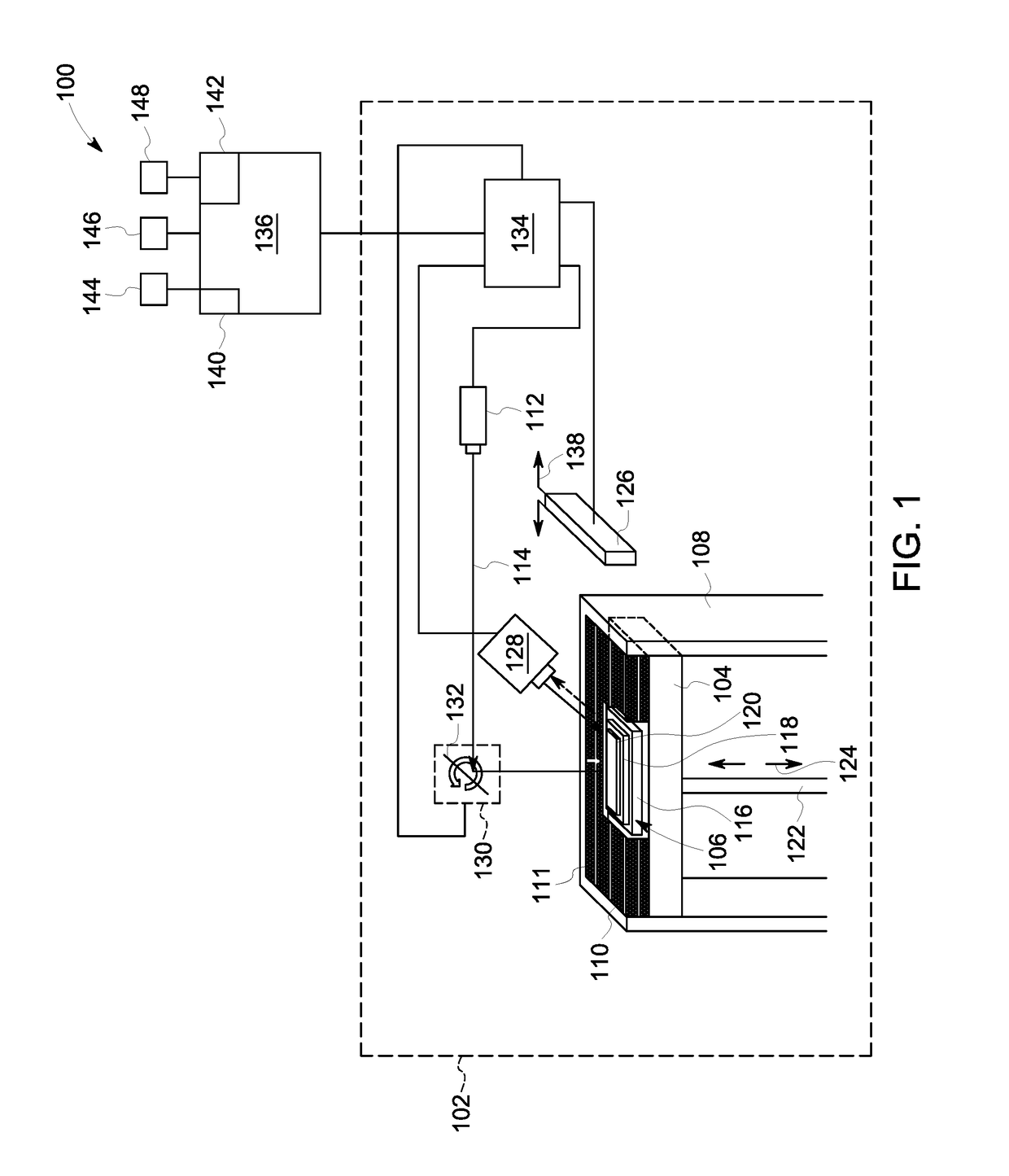
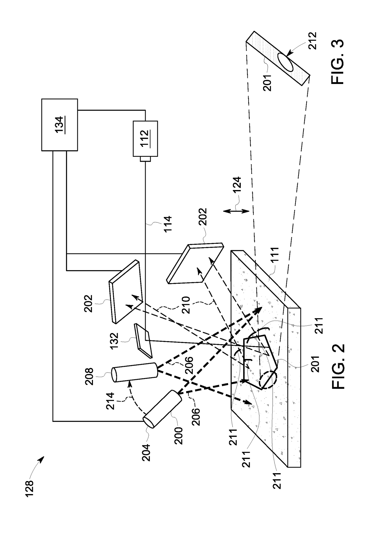
An additive manufacturing system includes at least one imaging device configured to direct electromagnetic radiation towards a build layer of a component positioned within a powder bed of the additive manufacturing system. The additive manufacturing system also includes at least one detector configured to detect the electromagnetic radiation that reflects from the build layer.

Description

CROSS REFERENCE TO RELATED APPLICATIONS[0001]This application claims priority to U.S. provisional patent application Ser. No. 62 / 445,064, filed Jan. 11, 2017, which is hereby incorporated by reference in its entirety.BACKGROUND[0002]The field of the disclosure relates generally to additive manufacturing systems and, more specifically, to imaging devices for use with additive manufacturing systems and methods of monitoring and inspecting additive manufacturing components.[0003]Additive manufacturing systems and processes are used to fabricate precision three-dimensional components from a digital model. Such components are fabricated using an additive process, where successive layers of material are solidified one on top of the other. At least some known additive manufacturing systems use a laser (or similar energy sources) and a series of lenses and mirrors to direct the laser over a powdered material in a pattern provided by a digital material. Some known additive manufacturing syst...

Claims


Application Information

Patent Timeline
Patent Type & Authority Applications(United States)
IPC IPC(8): B23K26/03B33Y10/00B33Y30/00B33Y40/00B23K26/342G01N23/04
CPCB23K26/032B33Y10/00B33Y30/00B33Y40/00B23K26/342G01N23/04G01N23/203B22F2203/11B33Y50/02Y02P10/25G01N25/72B22F12/44B22F10/28B22F10/38B22F12/49B22F12/45B22F12/41B22F10/366B22F12/90G05B19/4099
Inventor HARDING, KEVIN GEORGEROSS, WILLIAM ROBERTKNIGHT, BRYON EDWARDNALLADEGA, VENKATA VIJAYARAGHAVABUENO, CLIFFORD
Owner GENERAL ELECTRIC CO
Why Eureka
Try Eureka