Variable attenuator

Inactive Publication Date: 2018-08-23
SUMITOMO ELECTRIC DEVICE INNOVATIONS
View PDF1 Cites 1 Cited by
  • Summary
  • Abstract
  • Description
  • Claims
  • Application Information

AI Technical Summary

Benefits of technology

[0003]An aspect of the present invention relates to a variable attenuator (v-ATT) that includes an input terminal, an output terminal, a transmission line, first and second stages, and a bias unit. The input terminal receives a signal to be attenuated. The output terminal outputs an attenuated signal derived from the signal entering at the input terminal. The transmission line connects the input terminal with the output terminal and carries the attenuated signal thereon. The first and second stages are provided between the transmission line and he ground, each include a field effect transistor (FET) having a gate and two current terminals connected with the transmission line and the ground, respectively. The FET varies impedance between the two current terminals according to a bias supplied to the gate thereof. The bias unit includes an input and generates biases supplied to the first and second FETs in the first and second stages according to a control signal provided to the input of the bias unit. The bias unit supplies thus generated biases to the first and second stages. A feature of the present invention is that the biases supplied to the first and second stages are different from and independent each other.

Problems solved by technology

However, such a conventional v-ATT has shown response that a signal passing therethrough is distorted or increases higher order harmonics of the signal when a range of the attenuation is widened; that is, a conventional v-ATT has a subject that the range of the attenuation becomes a trade-off with respect to the signal distortion.

Method used


Image

  • Variable attenuator
  • Variable attenuator
  • Variable attenuator

Examples


first embodiment

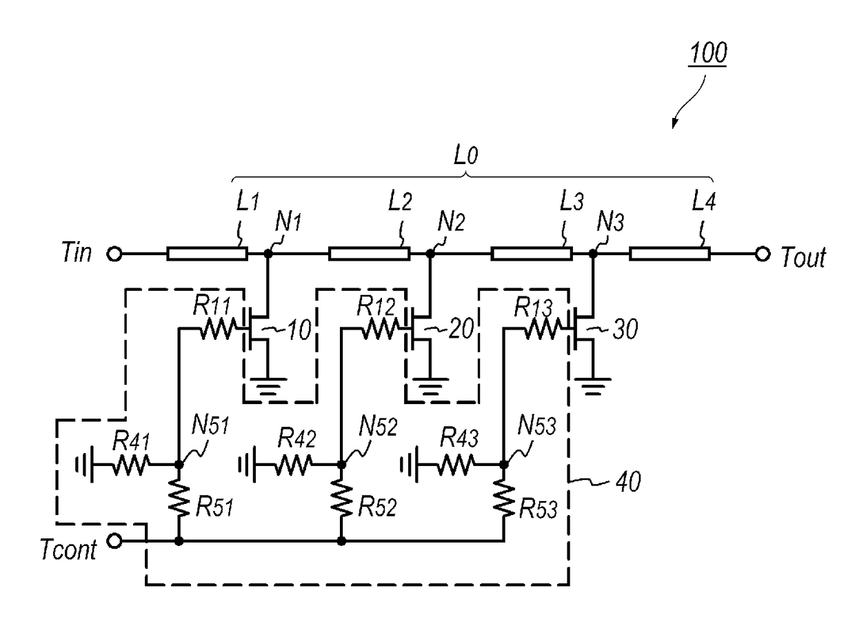
[0030]Next, a variable attenuator (v-ATT) according to the first embodiment of the present invention will be described. FIG. 1 shows a circuit diagram of the v-ATT 100 according to the first embodiment of the present invention. The v-ATT 100 includes, same with those implemented within the conventional v-ATTs, 200 and 200A, an input terminal Tin, an output Terminal Tout, transmission line L0 provided between the input terminal Tin and the output terminal Tout, three field effect transistors (FETs), 10 to 30, and a bias unit 40. Although the v-ATT 100 directly connects the transmission line L0 with the input terminal Tin and with the output terminal Tout, the transmission line L0 may be indirectly connected with those terminals, Tin and Tout, through capacitors that cut a DC component and low frequency components contained in a signal entering the input terminal Tin and to be attenuated.

[0031]The transmission line L0 includes four transmission line elements, L1 to L4, which interpose...

second embodiment

[0042]FIG. 4 shows a circuit diagram of another v-ATT according to the second embodiment of the present invention. The v-ATT 100A shown in FIG. 4 has a feature that FETs connected between the transmission line L0 and the ground have cascade connections. That is, two FETs, 10 and 12, with the cascade connection are provided between the intermediate node N1 and the ground. Two FETs, 20 and 22, also with the cascade connection are provided between the second intermediate node N2 and the ground. However, the FET 30 in the third stage, namely, the stage provided closest to the output terminal Tout, has the normal connection; that is no additional FET is connected in series with the third FET 30. The cascade connection of the FETs in the first and second stages means that one of the current nodes, the source, of the high side FET is directly connected with another of the current nodes, the drain, of the low side FET.

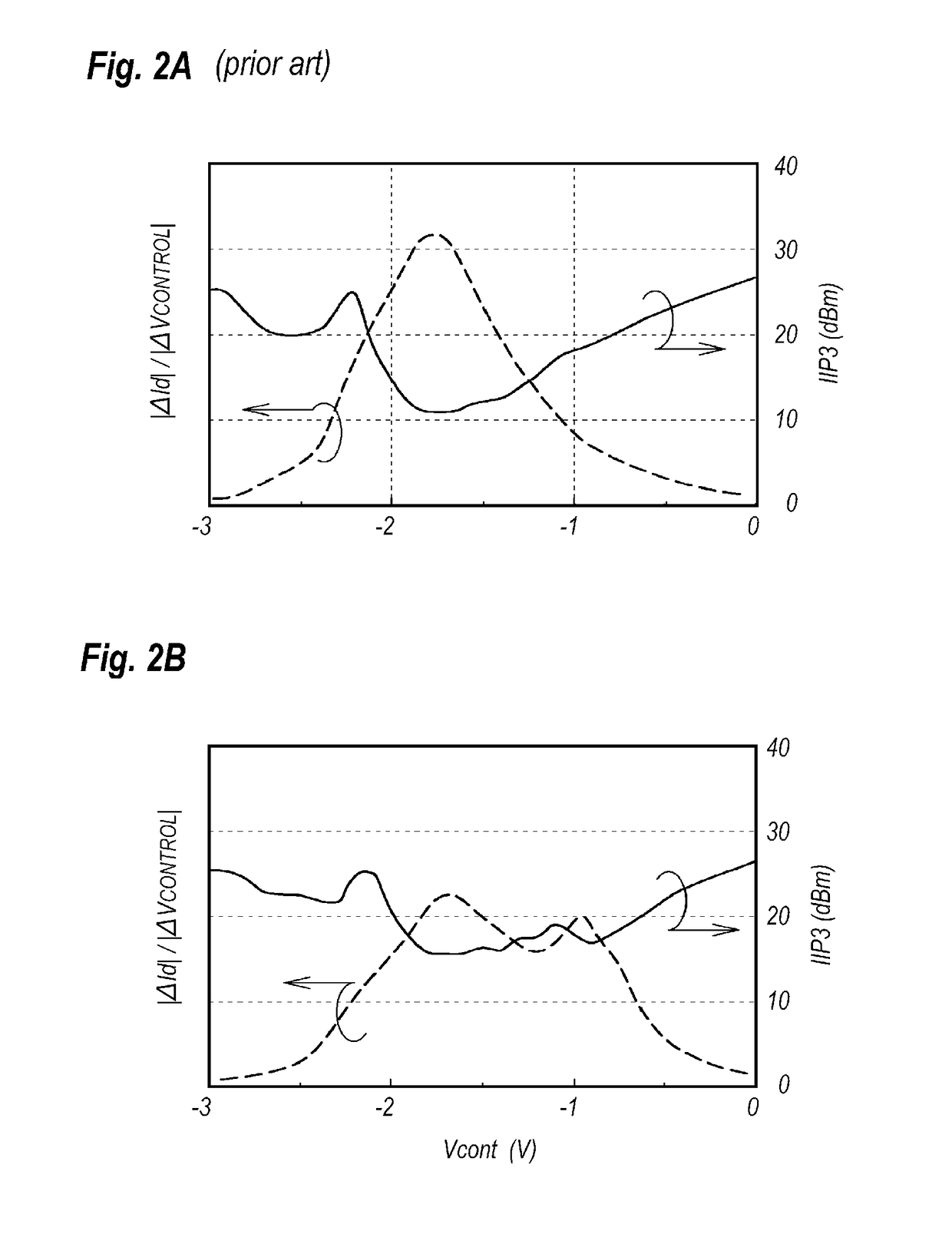
[0043]The distortion performance measured through the IIP3 and the attenu...

third embodiment

[0050]FIG. 6 shows a functional block diagram of an electronic apparatus according to the third embodiment of the present invention. The electronic apparatus 110 shown in FIG. 6 provides two v-ATTs, 100a and 100b, with a type of the first embodiment and / or the second embodiment, and two couplers, 54 and 56. Capacitors, C1 and C2, interposed between the input terminal T1 and the first coupler 54, and between the second coupler 56 and the output terminal T2, cut a DC component and low frequency components contained in the signal entering the input terminal T1. The coupler 54 divides a signal coming from the input terminal T1 into two portions having a phase difference of 90°, and provides thus divided two portions of the signal to the respective v-ATTs, 100a and 100b. The v-ATTs, 100a and 100b, attenuate the respective portions of the signal according to the control signal Vcont. The other coupler 56 mixes thus attenuated signals into one signal. Because the v-ATTs, 100a and 100b, cau...


PUM


Abstract

A variable attenuator (v-ATT) is disclosed. The v-ATT includes an input terminal, an output terminal, a transmission line between the input and output terminals, at least two stages provided between the transmission line and the ground, and a bias unit. Each of the stages includes a field effect transistor (FET) that varies impedance between the transmission line and the ground according to a bias provided to the gate thereof. The bias unit generates the biases each provided to the stages. One of the features of the v-ATT is that at least one of the stages receives at least one of the biases that is different from biases provided to other of the at least one of the stages.

Description

BACKGROUND OF INVENTION1. Field of Invention[0001]The present invention relates to a variable attenuator, in particular, relates to an attenuator for signal containing high frequency components and the attenuation thereof may be varied by a control signal.2. Related Background Arts[0002]A variable attenuator whose attenuation may be controlled by a control signal has been known in the field as a voltage variable attenuator (v-ATT). Japanese Patent Applications laid open No. JP-2000-124709A and JP-2009-200671A have disclosed such v-ATTs. However, such a conventional v-ATT has shown response that a signal passing therethrough is distorted or increases higher order harmonics of the signal when a range of the attenuation is widened; that is, a conventional v-ATT has a subject that the range of the attenuation becomes a trade-off with respect to the signal distortion.SUMMARY OF INVENTION[0003]An aspect of the present invention relates to a variable attenuator (v-ATT) that includes an inp...

Claims


Application Information

Patent Timeline
Patent Type & Authority Applications(United States)
IPC IPC(8): H03H11/24H01P1/22H03H7/25
CPCH03H11/245H01P1/22H03H7/253H03G1/0052H03G1/007H03G2201/106
Inventor OYA, AKIOKONDO, MAKOTO
Owner SUMITOMO ELECTRIC DEVICE INNOVATIONS
Why Eureka
Try Eureka