

Pixel structure and OLED display panel
a technology of organic light-emitting diodes and display panels, which is applied in the field of display technology, can solve the problems of significant power consumption of display panels, and the inability of conventional rgb pixel arrangements to meet the increasingly high ppi (pixels per inch) requirements, so as to increase the aperture ratio of sub-pixels, reduce process difficulty, and increase design margin
- Summary
- Abstract
- Description
- Claims
- Application Information
AI Technical Summary
Benefits of technology
Problems solved by technology
Method used
Image

Examples
embodiment 1
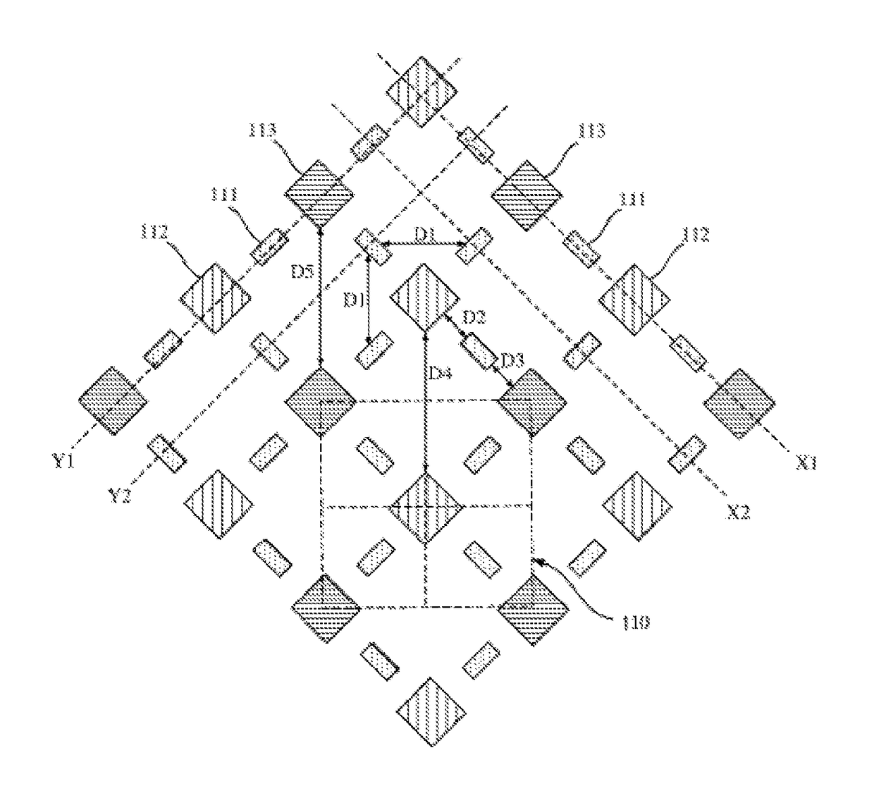
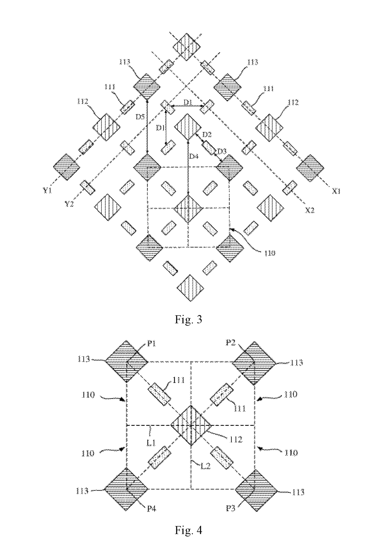
[0033]FIG. 3 is a schematic showing part of a pixel structure in an OLED display panel according to a first embodiment of the present invention. FIG. 4 is a schematic illustration of four pixel units in the pixel structure of FIG. 3.
[0034]As shown in FIGS. 3 to 4, the pixel structure of the OLED display panel includes a plurality of pixel units 110 arranged in an array, each comprising three sub-pixels including a first sub-pixel 111, a second sub-pixel 112 and a third sub-pixel 113. The first sub-pixel 111 is dedicated to the specific pixel unit 110, while the second and third sub-pixels 112, 113 are common to four adjacent pixel units. This arrangement enables, on the one hand, an increased aperture ratio of the sub-pixels and hence a longer life span of the display device at the same PPI and design margin, and on the other hand, an increased design margin and reduced process difficulty at the same PPI and aperture ratio because of expanded pixel-to-pixel spacings which are favora...
embodiment 2
[0044]FIG. 5 is a schematic showing part of a pixel structure in an OLED display panel according to a second embodiment of the present invention. FIG. 6 is a schematic illustration of four pixel units in the pixel structure of FIG. 5.
[0045]As shown in FIGS. 5 to 6, the pixel structure of the OLED display panel includes a plurality of pixel units 110 arranged in an array, each comprising three sub-pixels including a first sub-pixel 111, a second sub-pixel 112 and a third sub-pixel 113. The first sub-pixel 111 is dedicated to the specific pixel unit 110, while the second and third sub-pixels 112, 113 are common to four adjacent pixel units.
[0046]This embodiment differs from Embodiment 1 only in that the short sides of the first sub-pixel 111 are parallel to a line segment connecting centers of the second and third sub-pixels 112, 113, with its long sides extending perpendicular to this line segment, as shown in FIGS. 5 and 6.
embodiment 3
[0047]FIG. 7 is a schematic showing part of a pixel structure in an OLED display panel according to a third embodiment of the present invention. FIG. 8 is a schematic illustration of four pixel units in the pixel structure of FIG. 7.
[0048]As shown in FIGS. 7 to 8, the pixel structure includes a plurality of pixel units 110 arranged in an array, each comprising three sub-pixels including a first sub-pixel 111, a second sub-pixel 112 and a third sub-pixel 113. The first sub-pixel 111 is dedicated to the specific pixel unit 110, while the second and third sub-pixels 112, 113 are common to four adjacent pixel units.
[0049]This embodiment differs from Embodiment 1 only in that the first, second and third sub-pixels 111, 112, 113 are all squares so that the first, second and third sub-pixels 111, 112, 113 in one pixel unit is in exact symmetry to those in any adjacent pixel unit. Specifically, the first sub-pixels 111 in every two adjacent pixel units are in exact symmetry with respect to ...
PUM
 Abstract
Description
Claims
Application Information