Pixel circuit of display panel and display device

a display panel and display panel technology, applied in the direction of instruments, static indicating devices, etc., can solve the problems of color shift problem that a color is greatly changed for each grayscale, and the number of grayscales that can be expressed is limited, so as to achieve low color shift and high luminance uniformity

Active Publication Date: 2018-10-11
SAMSUNG ELECTRONICS CO LTD
View PDF3 Cites 39 Cited by
  • Summary
  • Abstract
  • Description
  • Claims
  • Application Information

AI Technical Summary

Benefits of technology

[0007]Example embodiments may overcome the above disadvantages and other disadvantages not described above, and provide a pixel circuit of a display panel having high luminance uniformity and low color shift and a display device.
[0027]According to example embodiments as described above, a pixel circuit of a display panel having high luminance uniformity and low color shift and a display device can be provided.

Problems solved by technology

However, in the case of the LED that is different from the OLED, a color shift phenomenon due to forward voltage (Vf) deviation between LEDs or the size of a drive current becomes greater than that of the OLED, and thus it is difficult to apply the AM driving circuit, which has been applied to the OLED display, to the LED display as it is.
Specifically, a pulse amplitude modulation (PAM) driving method in which an amplitude of a drive current differs for each grayscale for grayscale expression has been widely adopted in the OLED display, but if a PAM driving circuit in the related art is applied to the LED display as it is, a color shift problem that a color is greatly changed for each grayscale may occur.
Particularly, in the case of a digital PWM method, since grayscales are expressed in a sub field method, the number of grayscales that can be expressed is limited, and a false contour problem occurs.

Method used


Image

  • Pixel circuit of display panel and display device
  • Pixel circuit of display panel and display device
  • Pixel circuit of display panel and display device

Examples


Embodiment Construction

[0045]Hereinafter, example embodiments will be described in detail with reference to the accompanying drawings. In describing the present disclosure, related well-known technologies are not described in detail if they would obscure the subject matter of the present disclosure with unnecessary detail. Further, a suffix “unit” of a constituent element used in the following description may be given or mixedly used in consideration of easy preparation of the description only, but does not have any distinguishable meaning or role by itself.

[0046]The terms used in the description are used to merely describe example embodiments, but are not intended to limit and / or restrict the present disclosure. A singular expression may include a plural expression unless specially described on the context.

[0047]In the description, the term “includes” or “has” used in the description represents that features, figures, steps, operations, constituent elements, components, or combinations thereof exist, and...


PUM


Abstract

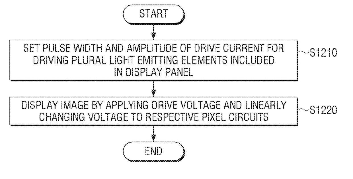
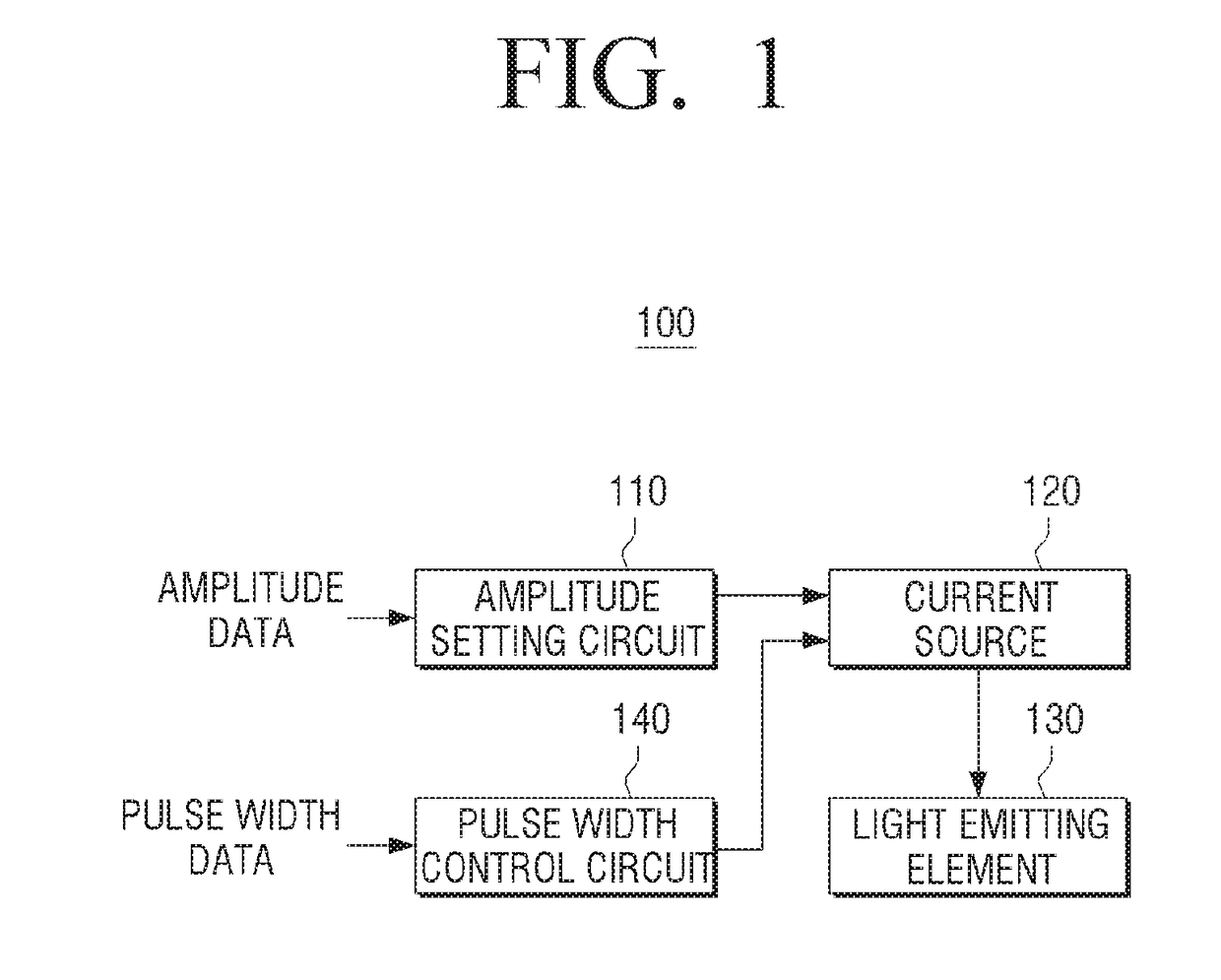
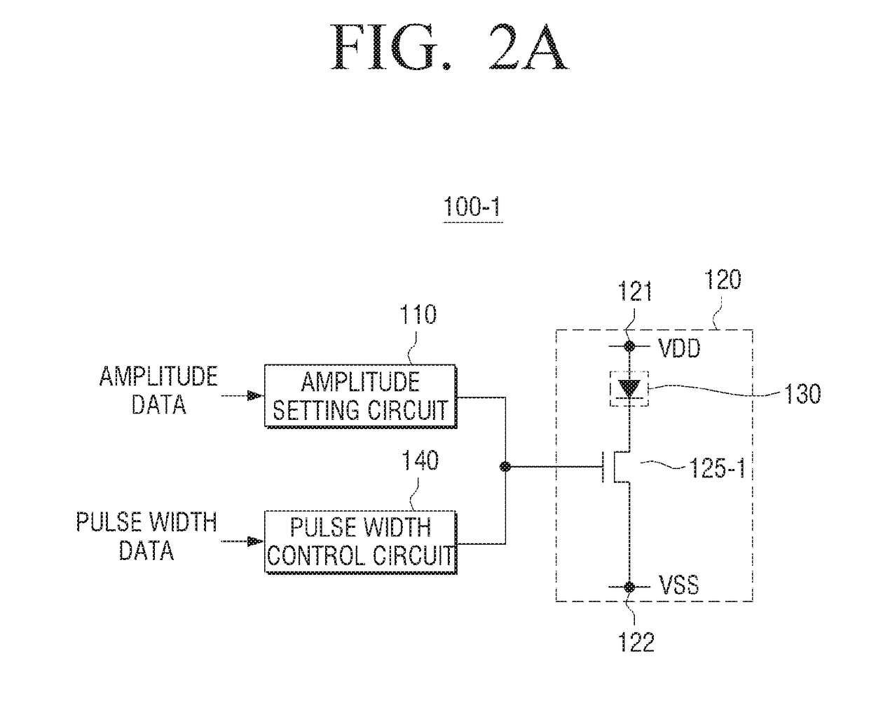
A pixel circuit of a display panel is provided, which includes a light emitting element configured to emit light in accordance with a drive current, a current source including a driving transistor connected to the light emitting element, and the current source is configured to provide the drive current having a different amplitude to the light emitting element in accordance with a level of a voltage applied to a gate terminal of the driving transistor, an amplitude setting circuit configured to apply a voltage having a different level to the gate terminal of the driving transistor, and a pulse width control circuit configured to control a duration of the drive current by controlling the voltage applied to the gate terminal of the driving transistor.

Description

CROSS-REFERENCE TO RELATED APPLICATIONS[0001]This application claims priority from Korean Patent Application No. 10-2017-0121742 filed on Sep. 21, 2017 in the Korean Intellectual Property Office, and the benefit of U.S. Provisional Patent Application No. 62 / 484,150 filed on Apr. 11, 2017 in the United States Patent and Trademark Office, the disclosures of which are incorporated herein by reference in their entireties.BACKGROUNDField[0002]The present disclosure relates to a pixel circuit of a display panel and a display device, and more particularly, to a pixel circuit of a display panel that expresses grayscales in accordance with an amplitude and a duration of a drive current and a display device.Description of the Related Art[0003]A light emitting diode (LED) display panel in the related art mainly adopts passive matrix (PM) driving, but active matrix (AM) driving is necessary for low power consumption. Recently, an AM driving circuit has been applied to an organic light emitting ...

Claims


Application Information

Patent Timeline
Patent Type & Authority Applications(United States)
IPC IPC(8): G09G3/20G09G3/3233
CPCG09G3/2081G09G3/3233G09G3/2011G09G2310/027G09G2310/0243G09G3/2018G09G2320/0233G09G2320/0242G09G2300/0819G09G2300/0852
Inventor SHIGETA, TETSUYAPARK, SANG-YOUNGLEE, HO-SEOP
Owner SAMSUNG ELECTRONICS CO LTD
Why Eureka
Try Eureka