Method of manufacturing semiconductor apparatus

Active Publication Date: 2018-11-15
CANON KK
View PDF5 Cites 0 Cited by
  • Summary
  • Abstract
  • Description
  • Claims
  • Application Information

AI Technical Summary

Benefits of technology

The patent text describes a method of manufacturing a semiconductor apparatus with two circuit sections. The method involves applying a photoresist to different parts of the member, exposing them with separate photomasks, and developing the photoresist to form resist patterns. The patterns are then used to etch the corresponding parts of the member. The technical effect of this method is to provide precise control over the patterning of the semiconductor apparatus, allowing for more complex and accurate circuit designs.

Problems solved by technology

Therefore, there is an issue that performance of a semiconductor apparatus as the photoelectric conversion apparatus is not sufficiently improved.

Method used


Image

  • Method of manufacturing semiconductor apparatus
  • Method of manufacturing semiconductor apparatus
  • Method of manufacturing semiconductor apparatus

Examples


Embodiment Construction

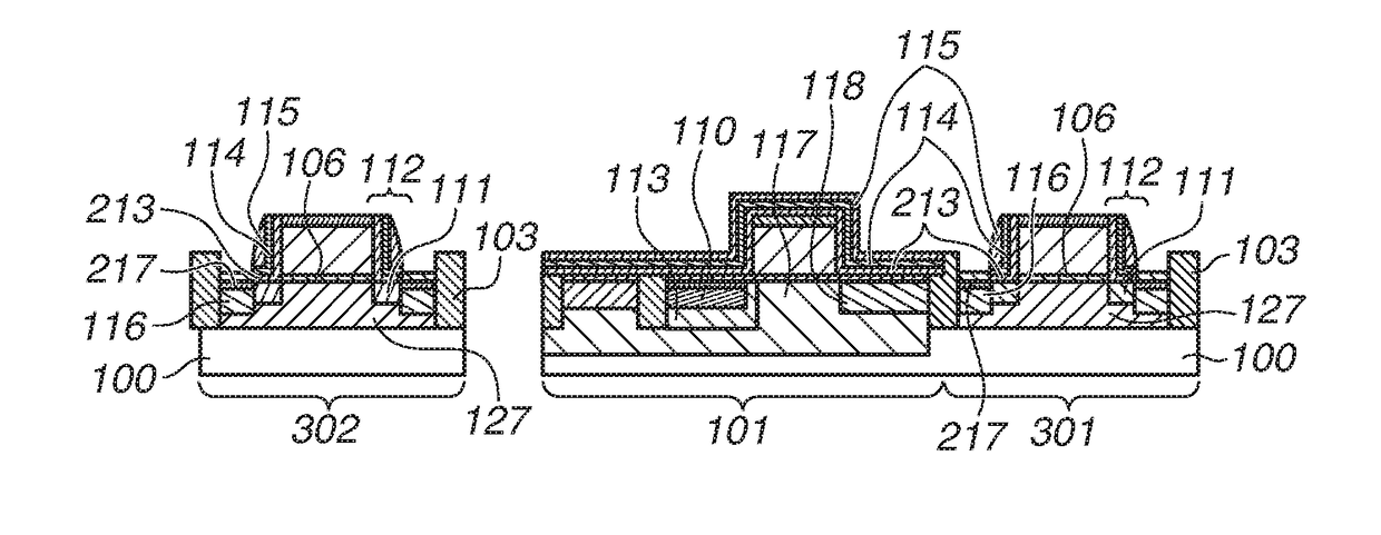
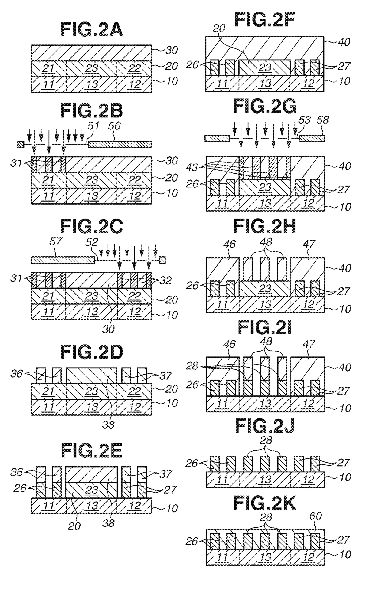
[0010]An exemplary embodiment of the disclosure is described below with reference to drawings. In the following description and drawings, a component common to a plurality of drawings is denoted by a common reference numeral. Accordingly, the common component is described with mutually referring the plurality of drawings, and description of the component denoted by the common reference numeral is appropriately omitted.

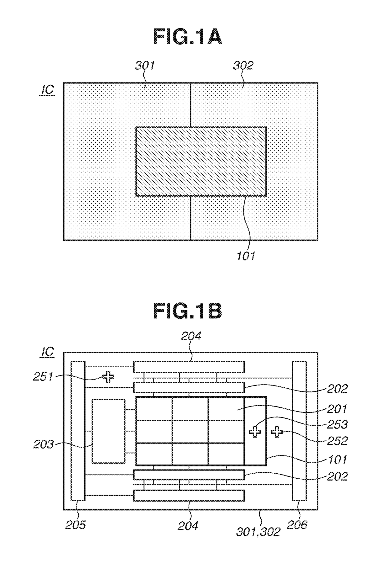
[0011]FIG. 1A is a schematic plan view of a photoelectric conversion apparatus IC. The photoelectric conversion apparatus IC is a semiconductor apparatus including at least a semiconductor chip. The semiconductor chip suitable in the present exemplary embodiment includes a quadrilateral shape in which a short side has a length larger than 26 mm and a long side has a length larger than 33 mm. The semiconductor chip more suitable in the present exemplary embodiment includes a quadrilateral shape in which a short side has a length equal to or larger than 30 mm and a long ...


PUM


Abstract

A method of manufacturing a semiconductor apparatus comprises forming a first photoresist on each of a first portion and a second portion of a member, exposing the first photoresist on the first portion using a first photomask, exposing the first photoresist on the second portion using a second photomask, forming a first resist pattern by developing the first photoresist on the first portion and the second portion, etching the first portion and the second portion using the first resist pattern as a mask, forming a second photoresist on a third portion of the member, exposing the second photoresist on the third portion using a third photomask, forming a second resist pattern by developing the second photoresist on the third portion, and etching the third portion using the second resist pattern as a mask.

Description

BACKGROUND OF THE INVENTIONField of the Invention[0001]The aspect of the embodiments relates to a method of manufacturing a semiconductor apparatus.Description of the Related Art[0002]In manufacturing a photoelectric conversion apparatus having a large size, an exposure region by photolithography is divided (hereinafter, referred to as “division exposure”), which makes it possible to manufacture a photoelectric conversion apparatus that includes an area larger than the maximum exposure range (screen size) of an exposure apparatus.[0003]Japanese Patent Application Laid-Open No. H11-220116 discusses a method of manufacturing a solid-state imaging device. The method includes performing exposure with use of a first photomask for a light receiving section and performing exposure with use of a second photomask for a peripheral circuit section.[0004]In Japanese Patent Application Laid-Open No. H11-220116, processing after the division exposure is not discussed in detail. The characteristic...

Claims


Application Information

Patent Timeline
IPC IPC(8): H01L21/28H01L21/3213H01L21/78H01L27/146
CPCH01L21/28123H01L21/32139H01L21/78H01L27/14683H01L21/3083H01L21/31144H01L21/32137H01L23/544H01L2223/54426H01L27/14612H01L27/14689H01L27/146
Inventor ENDO, NOBUYUKI
Owner CANON KK
Why Eureka
Try Eureka