Optical element and manufacturing method thereof and optical modulator

a manufacturing method and optical modulator technology, applied in the field of optical elements, can solve the problems of large fundamental mode loss and difficulty in suppressing a higher order horizontal mode, and achieve the effect of suppressing the fundamental mode loss to, reducing or eliminating the higher order mode, and low level

Active Publication Date: 2018-11-22
FURUKAWA ELECTRIC CO LTD
View PDF20 Cites 9 Cited by
  • Summary
  • Abstract
  • Description
  • Claims
  • Application Information

AI Technical Summary

Benefits of technology

[0015]According to the present invention, it is possible to sufficiently reduce or remove a higher order mode while suppressing the fundamental mode loss to a low level. Further, according to the present invention, an optical element that can sufficiently reduce or remove a higher order mode while suppressing the fundamental mode loss to a low level can be easily manufactured at low cost.

Problems solved by technology

A high-mesa structured optical waveguide has a significantly narrow cutoff mesa width, which makes it difficult to suppress a higher order horizontal mode.
On the other hand, in a high-mesa structured optical waveguide, an excessively narrow mesa width for increasing a higher-order mode loss causes a larger fundamental mode loss.

Method used


Image

  • Optical element and manufacturing method thereof and optical modulator
  • Optical element and manufacturing method thereof and optical modulator
  • Optical element and manufacturing method thereof and optical modulator

Examples


first embodiment

[0051]An optical element and a manufacturing method thereof according to a first embodiment of the present invention will be described by using FIG. 1 to FIG. 13.

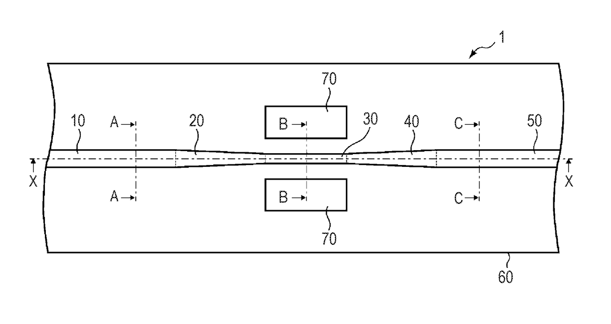
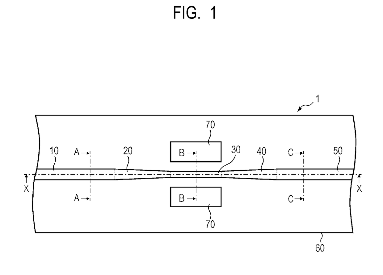
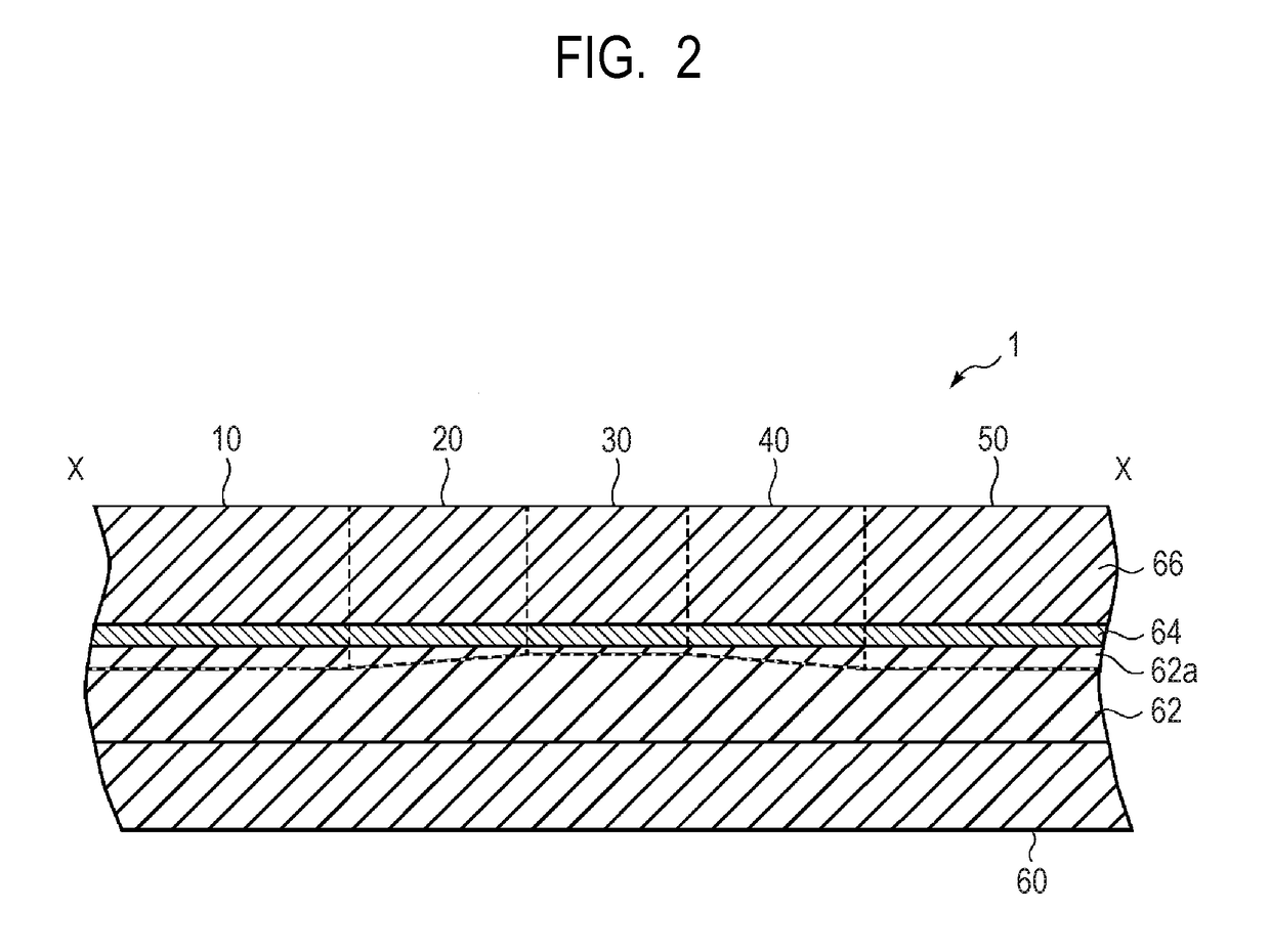
[0052]First, a configuration of the optical element according to the present embodiment will be described by using FIG. 1 to FIG. 4B. FIG. 1 is a plan view illustrating an optical element according to the present embodiment. FIG. 2 is a sectional view taken along the line X-X of FIG. 1. FIG. 3A is a sectional view taken along the line A-A of FIG. 1. FIG. 3B is a sectional view taken along the line B-B of FIG. 1. FIG. 3C is a sectional view taken along the line C-C of FIG. 1. FIG. 4A and FIG. 4B are sectional views illustrating another example of a sectional shape that may be included in the high-mesa structure of an optical waveguide.

[0053]The optical element according to the present embodiment functions as a higher order mode filter. The optical element according to the present embodiment can be integrated on a semiconduct...

second embodiment

[0127]An optical element and a manufacturing method thereof according to a second embodiment of the present invention will be described by using FIG. 14. FIG. 14 is a sectional view illustrating the third optical waveguide in the optical element according to the present embodiment. Note that the same components as those in the optical element and the manufacturing method thereof according to the first embodiment described above are labeled with the same reference numerals, and the description thereof will be omitted or simplified.

[0128]The basic configuration of the optical element according to the present embodiment is substantially the same as the configuration of the optical element 1 according to the first embodiment. The optical element according to the present embodiment has the high-mesa structure in which the third optical waveguide 30 is formed in a mesa shape from the upper clad layer 66 to the upper part of the core layer 64. In this regard, the optical element according ...

third embodiment

[0135]An optical modulator according to a third embodiment of the present invention will be described by using FIG. 15A and FIG. 15B. FIG. 15A and FIG. 15B are schematic diagrams illustrating the optical modulator according to the present embodiment. Note that the same components as those in the optical element and the manufacturing method thereof according to the first and second embodiments described above are labeled with the same reference numerals, and the description thereof will be omitted or simplified.

[0136]The optical element according to the first and second embodiments described above can be integrated on a semiconductor substrate together with an active element such as an optical modulator and other elements to form an optical integrated element. In the present embodiment, an example of such an optical integrated element will be described. Specifically, the optical modulator according to the present embodiment is a Mach-Zehnder optical modulator and has a plurality of t...


PUM

PropertyMeasurementUnit
thicknessaaaaaaaaaa
thicknessaaaaaaaaaa
distanceaaaaaaaaaa

Abstract

An optical element has a substrate; and first to third optical waveguides formed on the substrate and each having a lower clad layer, a core layer, and an upper clad layer, the core layer having a larger refractive index than the lower clad layer and the upper clad layer. The first optical waveguide is optically connected to the second optical waveguide, and the second optical waveguide is optically connected to the third optical waveguide. The first to third optical waveguides have a mesa structure formed in a mesa shape in which at least the upper clad layer and an upper part of the core layer project above the lower clad layer. The core height of the third optical waveguide is lower than the core height of the first optical waveguide. The mesa width of the third optical waveguide is narrower than the mesa width of the first optical waveguide.

Description

CROSS-REFERENCE TO RELATED APPLICATIONS[0001]This application is a continuation application of International Application No. PCT / JP2017 / 004058, filed Feb. 3, 2017, which claims the benefit of Japanese Patent Application No. 2016-019876, filed Feb. 4, 2016. The contents of the aforementioned applications are incorporated herein by reference in their entireties.TECHNICAL FIELD[0002]The present invention relates to an optical element having an optical waveguide and a manufacturing method thereof.BACKGROUND ART[0003]As one of optical waveguides, a semiconductor optical waveguide having a core layer and a clad layer made of a semiconductor material formed on a semiconductor substrate is known. As waveguide structure of a semiconductor optical waveguide in an optical functional element or the like, the structure called high-mesa structure may be employed, for example. A high-mesa structured optical waveguide is featured in a small waveguide loss and ability of reducing a bending radius.[0...

Claims


Application Information

Patent Timeline
Patent Type & Authority Applications(United States)
IPC IPC(8): G02B6/122G02B6/136G02F1/225
CPCG02B6/1228G02B6/136G02F1/2257G02B2006/12173G02F2001/212G02B2006/12078G02F1/025G02B6/14G02F1/212
Inventor SAITO, YUSUKEKIMOTO, TATSUYA
Owner FURUKAWA ELECTRIC CO LTD
Why Eureka
Try Eureka