

Composition for polishing semiconductor layers
a technology for semiconductor layers and compositions, applied in the direction of silicon compounds, lapping machines, other chemical processes, etc., can solve the problems of low k dielectrics at unacceptable removal rates, detrimental to the ultimate performance of the integrated circuit, and not showing the selectivity requisite for silicon oxide-containing layers, etc., to achieve the effect of reducing defectivity
- Summary
- Abstract
- Description
- Claims
- Application Information
AI Technical Summary
Benefits of technology
Problems solved by technology
Method used
Image

Examples
example 1
The PL150H25 is a colloidal silica from Clariant, having 30 wt % silica particles with an average particle size of 25 nm.
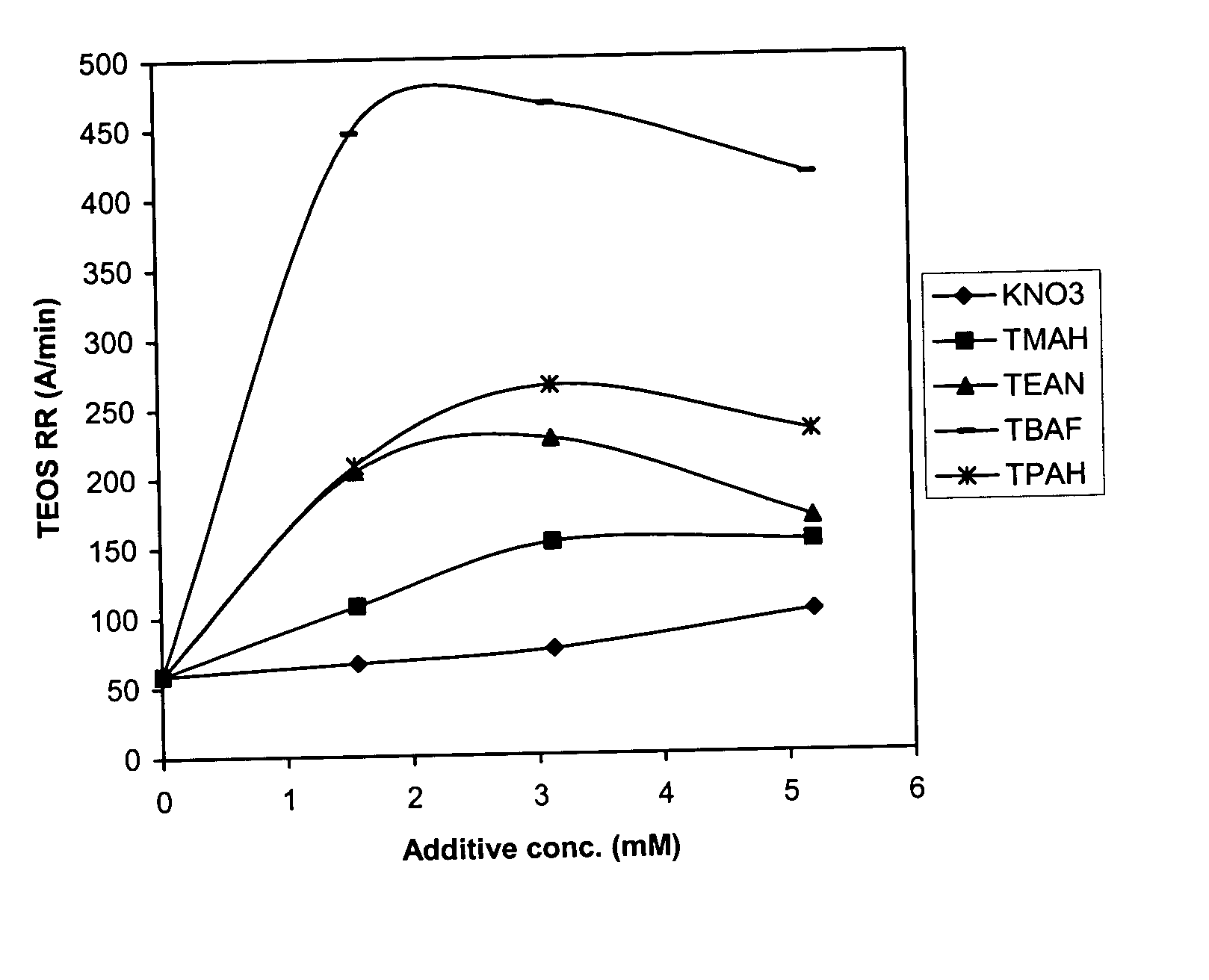
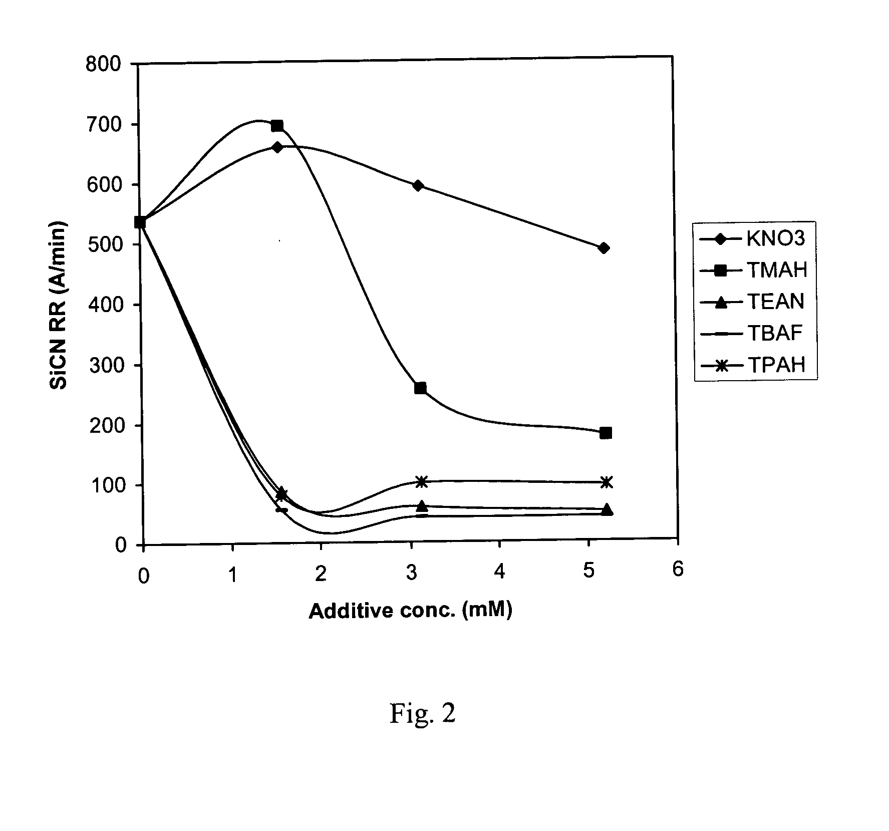
This experiment was conducted to determine the polishing performance of the polishing composition at varying component concentrations. Polishing experiments were performed using a Mirra® model polishing equipment supplied by Applied Materials. The polishing pad was an IC1010™ porous-filled polyurethane polishing pad supplied by Rodel, Inc. The pad was conditioned prior to each run. The polishing process was performed at a pressure of 6.9 kPa (1 psi), a table speed of 120 revolutions per minute (rpm) and a carrier speed of 114 rpm. The polishing composition supply rate was 180 ml / min.
It is to be noted in the following examples, that letters of the alphabet identify the comparative compositions, whereas the examples representing the polishing compositions are identified numerically. In this example, tetramethylammonium hydroxide and potassium nitrate were used ...
example 2
This example was conducted to further demonstrate that the high TEOS removal rate was not caused by the fluoride ion in the TBAF additive slurries. In this example, the comparative compositions H, I, and J comprise a fluoride ion. The fluoride ion was added to the polishing composition in the form of ammonium fluoride (NH4F). As mentioned in example 1, comparative composition A contained the control formulation without any fluoride ion. The polishing composition is represented by Sample #10, which contained tetrabutylammonium fluoride. The polishing conditions were similar to those in Example 1. The formulations are shown in Table 2.
TABLE 2Addition byAddition byTaNCuTEOSSICNCDOSampleAdditivemMwt. %RRRRRRRRRRA65310941614138HNH4F1.56 mM0.00578%107410867648163INH4F3.12 mM 0.0116%7859573376171JNH4F5.21 mM 0.0193%793978127213310TBAF1.56 mM 0.0492%816725187877
The above data show quite conclusively that the samples that contain the ammonium fluoride do not display a high TEOS removal r...
example 3
This example was conducted to determine the effect of different ions on the removal rate of TEOS masks of the integrated circuit. Polishing experiments were performed using a Mirra model polishing equipment supplied by Applied Materials. The polishing pad was a Politex™ pad supplied by Rodel, Inc. The pad was conditioned prior to each run. The polishing process was performed at a membrane pressure of 10.33 kPa (1.5 psi), a table speed of 93 revolutions per minute (rpm) and a carrier speed of 87 rpm. The polishing composition supply rate was 180 m / min.
In this experiment, Sample A represents the control composition, while Samples 11-16 utilizing tetrabutylammonium nitrate and Samples 17-22 utilizing tetrabutylammonium fluoride represent the polishing compositions. The respective experimental compositions along with the results are shown in Table 3 below.
TABLE 3TBANTBANTBAFTBAFSamplemMwt %mMwt %TaN RRCu RRTEOS RRSiCN RRCDO RRA145318681795238110.3170.00965134684131654441120.9510.02...
PUM
| Property | Measurement | Unit |
|---|---|---|
| Pressure | aaaaa | aaaaa |
| Acidity | aaaaa | aaaaa |
| Molar density | aaaaa | aaaaa |
Abstract
Description
Claims
Application Information