Wafer producing apparatus

a technology of producing apparatus and wafer, which is applied in the direction of laser beam welding apparatus, manufacturing tools, welding/soldering/cutting articles, etc., can solve the problems of reducing production efficiency and achieve the effect of improving production efficiency

Active Publication Date: 2018-12-13
DISCO CORP
View PDF0 Cites 9 Cited by
  • Summary
  • Abstract
  • Description
  • Claims
  • Application Information

AI Technical Summary

Benefits of technology

[0009]According to the wafer producing apparatus of the present invention, the wafer can be automatically produced from the ingot and then stored into the wafer storing unit. Accordingly, the production efficiency can be improved.

Problems solved by technology

However, the step of forming the separation layer inside the SiC ingot, the step of separating the SiC wafer from the SiC ingot, and the step of grinding the upper surface of the SiC ingot to thereby flatten the upper surface of the SiC ingot are all performed manually, causing a reduction in production efficiency.

Method used


Image

  • Wafer producing apparatus
  • Wafer producing apparatus
  • Wafer producing apparatus

Examples


Embodiment Construction

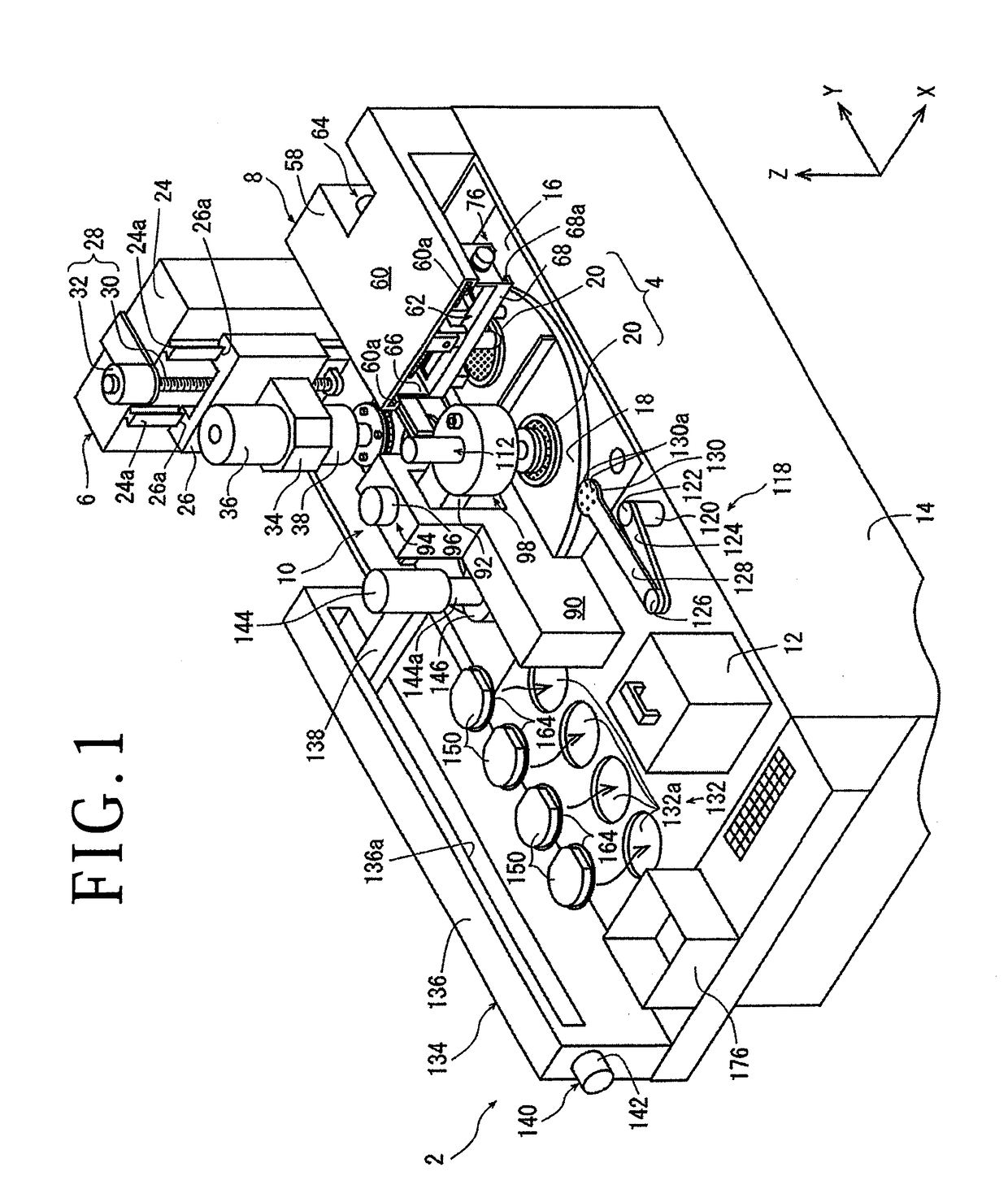
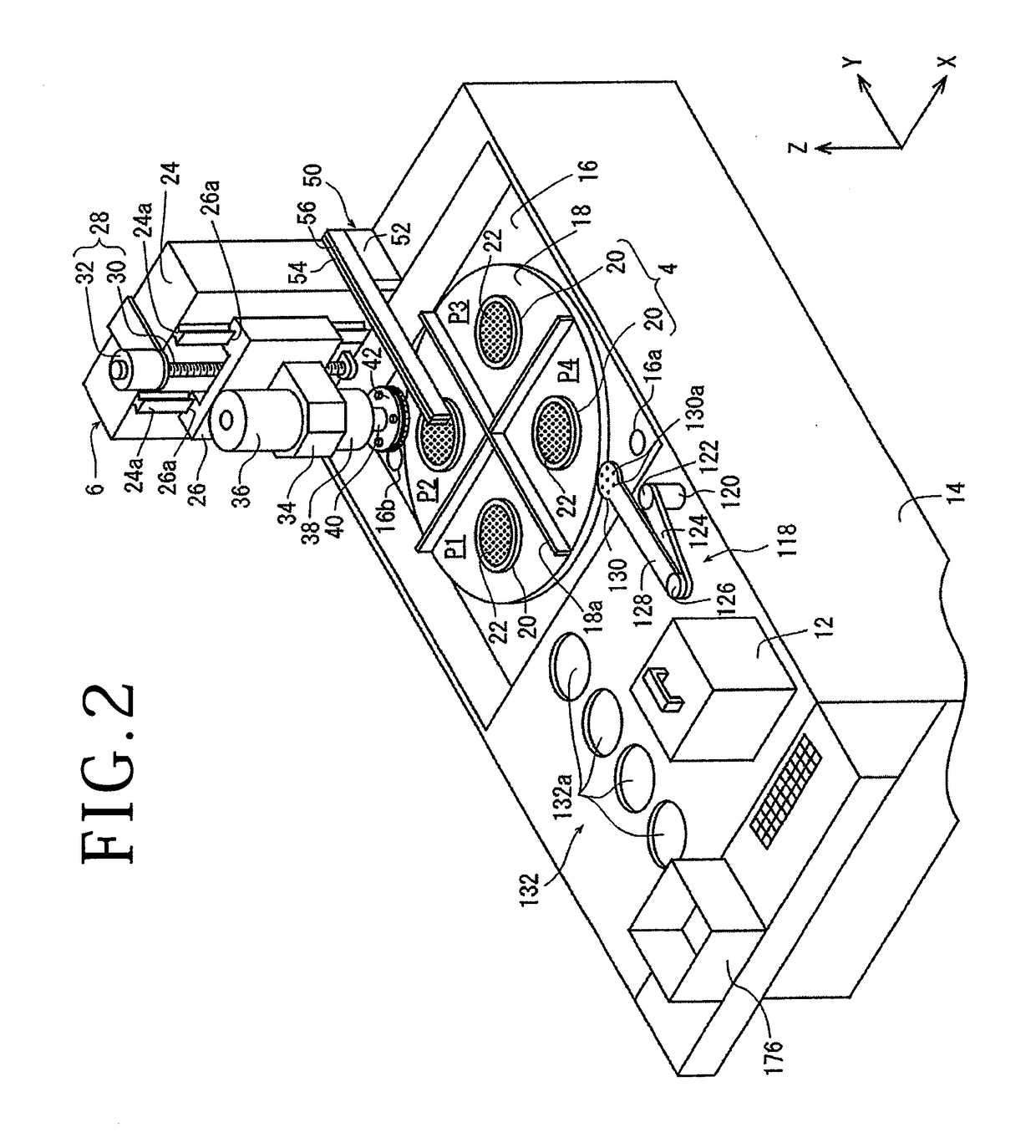
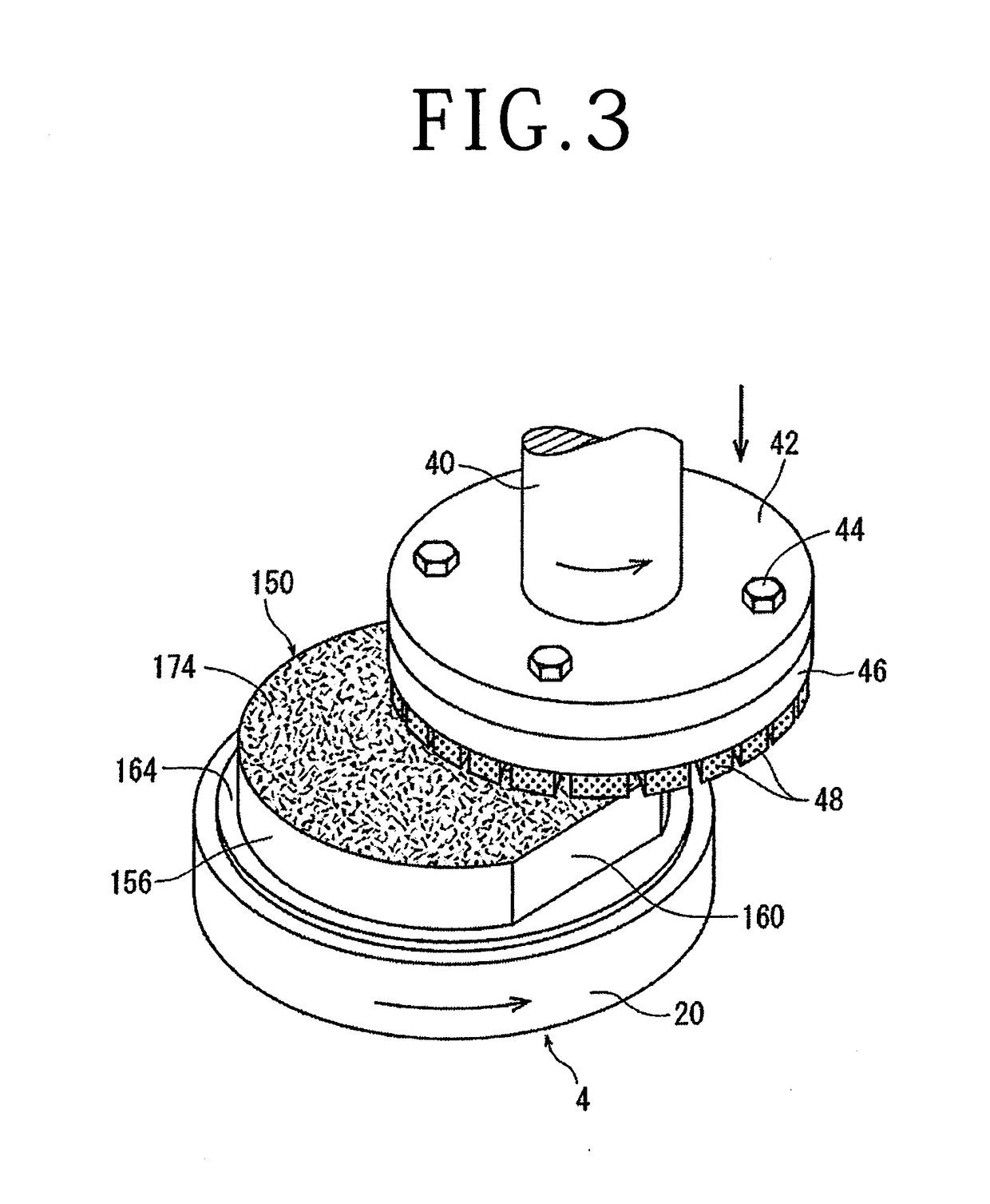
[0039]A preferred embodiment of the wafer producing apparatus according to the present invention will now be described with reference to the drawings. FIG. 1 shows a wafer producing apparatus 2 according to this preferred embodiment. The wafer producing apparatus 2 includes a holding unit 4 for holding a single crystal SiC ingot (which will be hereinafter referred to simply as “ingot”), a flattening unit 6 for grinding the upper surface of the ingot held by the holding unit 4, thereby flattening the upper surface of the ingot, a laser applying unit 8 for setting the focal point of a laser beam having a transmission wavelength to the ingot inside the ingot at a predetermined depth from the upper surface of the ingot held by the holding unit 4, the predetermined depth corresponding to the thickness of an SiC wafer to be produced (which will be hereinafter referred to simply as “wafer”), and next applying the laser beam to the ingot to thereby form a separation layer for separating the...


PUM

PropertyMeasurementUnit
depthaaaaaaaaaa
Feed speedaaaaaaaaaa
roughnessaaaaaaaaaa

Abstract

A SiC wafer is produced from a single crystal SiC ingot. Wafer producing apparatus includes a holding unit for holding the ingot, a flattening unit for grinding the upper surface of the ingot, thereby flattening the upper surface, a laser applying unit for setting the focal point of a laser beam having a transmission wavelength to the ingot inside the ingot at a predetermined depth from the upper surface of the ingot, the predetermined depth corresponding to the thickness of the wafer to be produced, and next applying the laser beam to the ingot to thereby form a separation layer for separating the wafer from the ingot, a wafer separating unit for holding the upper surface of the ingot to separate the wafer from the ingot along the separation layer, and a wafer storing unit for storing the wafer separated from the ingot.

Description

BACKGROUND OF THE INVENTIONField of the Invention[0001]The present invention relates to a wafer producing apparatus for producing an SiC wafer from a single crystal SiC ingot.Description of the Related Art[0002]Various devices such as integrated circuits (ICs), large scale integrated circuits (LSIs), and light emitting diodes (LEDs) are formed by forming a functional layer on the front side of a wafer formed of Si (silicon) or Al2O3 (sapphire) and partitioning this functional layer into a plurality of separate regions along a plurality of division lines. Further, power devices or optical devices such as LEDs are formed by forming a functional layer on the front side of a wafer formed of single crystal SiC (silicon carbide) and partitioning this functional layer into a plurality of separate regions along a plurality of division lines. The division lines of such a wafer having these devices are processed by a processing apparatus such as a cutting apparatus and a laser processing appa...

Claims


Application Information

Patent Timeline
Patent Type & Authority Applications(United States)
IPC IPC(8): B23K26/00
CPCH01L29/1608B23K2103/56B23K26/53B23K26/0006H01L21/02008H01L21/02041H01L21/02002H01L21/67092H01L21/67028B23K26/38H01L21/02378H01L21/02686
Inventor IIZUKA, KENTAROOMIYA, NAOKIMORI, TAKASHIYAMANAKA, SATOSHIHIRATA, KAZUYA
Owner DISCO CORP
Why Eureka
Try Eureka