Print element substrate, method of manufacturing print element substrate, and method of manufacturing printhead

a printing element and substrate technology, applied in the direction of printing, inking apparatus, etc., can solve the problems of large influence of wiring resistance variation, difficult high-quality printing, and large density unevenness, so as to suppress the deviation of heater size, suppress the variation of wiring resistance value, and suppress the effect of density unevenness between the print element substrates

Active Publication Date: 2019-01-03
CANON KK
View PDF1 Cites 0 Cited by
  • Summary
  • Abstract
  • Description
  • Claims
  • Application Information

AI Technical Summary

Benefits of technology

[0010]According to the present invention, it is possible to suppress a variation in the resistance values of wirings connected to the resistance monitor elements and suppress a deviation of heater sizes calculated from the resistance values. Accordingly, in the printhead in which the plurality of print element substrates are arranged, density unevenness between the print element substrates can be suppressed, and satisfactory printing can be performed.

Problems solved by technology

However, following problems arise in a printhead having such an arrangement.
When printing is performed using a printhead in which such print element substrates are arranged, even a small discharge amount difference between the print element substrates causes density unevenness, resulting in difficulty in performing high-quality printing.
In particular, if the discharge amount difference is large between adjacent print element substrates, the density unevenness is very noticeable.
In particular, if the sheet resistance values of the heater and the test resistor are low, the influence of the variation in the wiring resistance becomes large.

Method used


Image

  • Print element substrate, method of manufacturing print element  substrate, and method of manufacturing printhead
  • Print element substrate, method of manufacturing print element  substrate, and method of manufacturing printhead
  • Print element substrate, method of manufacturing print element  substrate, and method of manufacturing printhead

Examples


first embodiment

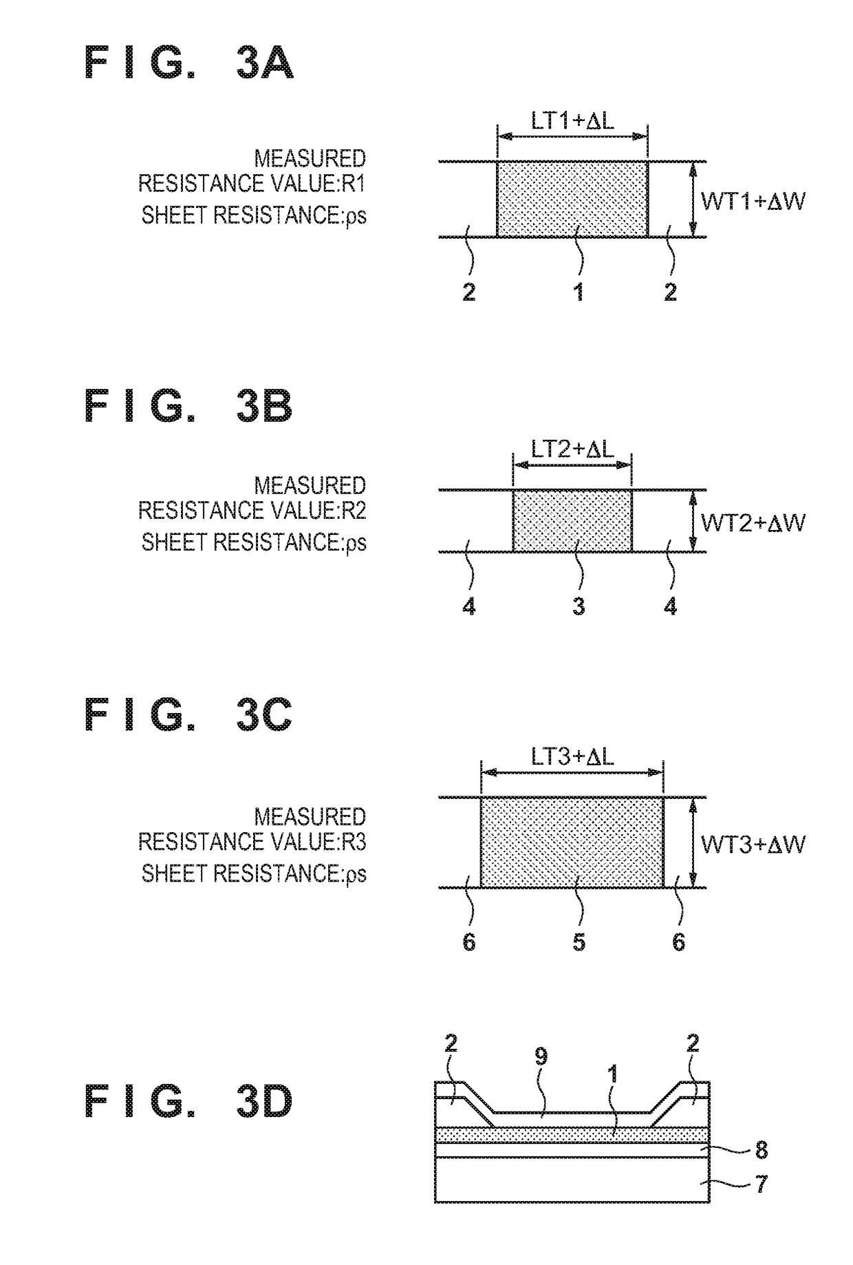
[0044]A case in which the three types of resistance monitor elements shown in FIGS. 3A to 3D are used will be described. Note that the number of resistance monitor elements is merely an example and is not limited to this number.

[0045]FIG. 3A shows a resistor 1 as a first resistance monitor element and electrodes 2 connected to this. The width of the resistor 1 is represented by WT1 +ΔW, and the length is represented by LT1+ΔL. WT1 and LT1 are the design value of the width and the design value of the length of the first resistance monitor element. In addition, ΔW and ΔL are the deviation amount of the width and the deviation amount of the length of the resistor from the design values at the time of formation. The sheet resistance value of the resistor 1 is ps, and the resistance value of the first resistance monitor element is R1. Note that the width of the resistor 1 is the length of the resistor 1 in the direction orthogonal to the direction in which a current flows in the resistor...

second embodiment

[0084]FIGS. 8A, 8B, 8C, and 8D are views showing examples of the arrangements of resistance monitor elements according to the second embodiment of the present invention. This is an example of a case in which the layers of the resistance elements are made flat using a planarization technique.

[0085]FIG. 8A shows a resistor 11 serving as a first resistance monitor element, electrodes 12, and a plurality of vias 13 that electrically connect the resistor 11 and the electrodes 12. FIG. 8B shows a resistor 14 serving as a second resistance monitor element, electrodes 15, and the vias 13 that electrically connect the resistor 14 and the electrodes 15. FIG. 8C shows a resistor 16 serving as a third resistance monitor element, electrodes 17, and the vias 13 that electrically connect the resistor 16 and the electrodes 17. Note that in the resistance monitor element according to this embodiment, since a current flows to a portion of the resistor located between the plurality of pairs of vias 13...

third embodiment

[0091]FIGS. 9A, 9B, and 9C are views showing examples of the arrangements of resistance monitor elements according to the third embodiment of the present invention. This is an example of a case in which the connection method for the resistors of the resistance monitor elements is changed.

[0092]FIG. 9A shows a resistor 91 serving as a first resistance monitor element, and electrodes 92 connected to the resistor 91. The width of the resistor 91 is represented by WT4+ΔW, and the length is represented by LT4+ΔL. WT4 and LT4 are the design value of the width and the design value of the length of the first resistance monitor element. In addition, ΔW and ΔL are the deviation amount of the width and the deviation amount of the length of the resistor from the design values at the time of formation. The sheet resistance value of the resistor 91 is ps, and the resistance value of the first resistance monitor element is R4.

[0093]FIG. 9B shows resistors 93 serving as second resistance monitor el...


PUM


Abstract

A print element substrate comprises: a plurality of heaters configured to cause discharge of droplets; a pad array in which a plurality of pads configured to do electrical connection from an outside are arranged; and a plurality of resistance monitor elements configured to measure resistance values of the plurality of heaters, wherein the plurality of resistance monitor elements are arranged along a direction of the pad array.

Description

BACKGROUND OF THE INVENTIONField of the Invention[0001]The present invention relates to a print element substrate, a method of manufacturing a print element substrate, and a method of manufacturing a printhead.Description of the Related Art[0002]Conventionally, concerning an inkjet printing apparatus, there is known an apparatus that heats a liquid by an electrothermal transducer including a heater as an energy generation element configured to generate energy used to discharge ink from an orifice of a printhead.[0003]In recent years, to implement printing of a high-definition image at a higher speed, implementation of a printhead with a larger print width is demanded. More specifically, a printhead having a length of 4 inches to 12 inches is also required. An arrangement is known in which a plurality of print element substrates with nozzles, each of which includes an appropriate number of nozzles and has an appropriate length, are arranged on a plate, thereby implementing a printhea...

Claims


Application Information

Patent Timeline
Patent Type & Authority Applications(United States)
IPC IPC(8): B41J2/045B41J2/16
CPCB41J2/0451B41J2/1626B41J2/0458B41J2/1601B41J2/04565B41J2/1412B41J2/14129B41J2/14153B41J2202/18B41J2202/20B41J2202/21
Inventor TAMURA, HIDEOYAMAGUCHI, TAKAAKIOSUKI, YOHEI
Owner CANON KK
Why Eureka
Try Eureka