
Electro-optical device and electronic apparatus

a technology of optical devices and electronic devices, applied in the direction of electrical devices, semiconductor devices, diodes, etc., can solve the problems of deterioration of pixel deterioration, easy visible brightness unevenness in the pixel, and varies the life of the pixel, so as to improve the brightness unevenness

Active Publication Date: 2019-01-03
SEIKO EPSON CORP
View PDF5 Cites 17 Cited by
  • Summary
  • Abstract
  • Description
  • Claims
  • Application Information

AI Technical Summary

Benefits of technology

This patent describes a technique for improving brightness unevenness in a display device by adjusting the brightness of light emitted from different pixels. By making changes to the width of the light emitting region, the device can ensure that the brightness of each pixel is balanced when viewing it from a distance. This technique helps to reduce the effect of voltage differences on brightness and can improve the overall quality of color display. Additionally, the patent takes into account the fact that light emitted from pixels may have different wavelengths, and can use a second color filter to increase the efficiency of blue light shielding. This helps to maintain the brightness of each pixel and enhance the overall display quality.

Problems solved by technology

There has been a problem that the lifetime of the pixels varies due to the difference in the current values.
It is because the larger the current flows in the light emitting element, the more easily the pixel deteriorates.
For this reason, there has been a problem that brightness unevenness is easily visible in the pixel (for example, pixel R) having the lowest current value of the current to be supplied to the light emitting element.

Method used


Image

  • Electro-optical device and electronic apparatus
  • Electro-optical device and electronic apparatus
  • Electro-optical device and electronic apparatus

Examples


embodiment

3. Effect of Embodiment

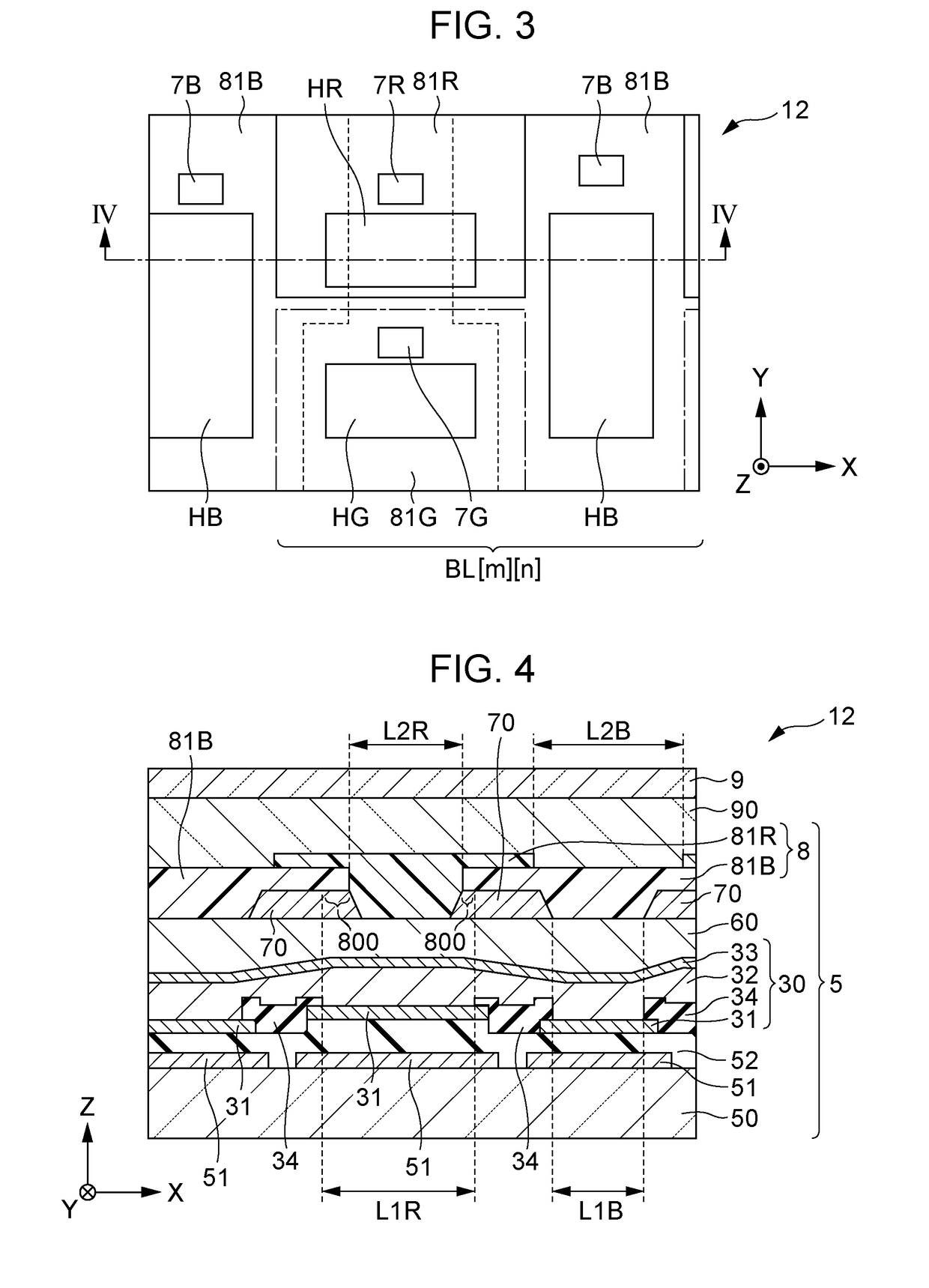
[0087]In the embodiment, assuming that area of the display surface of the display unit 12 as S, the area of the light emitting region HR as SR, the light emitting brightness of the light emitting region HR as LR1, and the opening ratio of the pixel PxR as T, the brightness LR at the time of viewing the light emitting region HR from a distance is expressed by the following Equation (3).

LR=LR1×T×SR / S   (3)

[0088]According to the embodiment, by decreasing T, it is possible to increase the light emitting brightness LR1 of light emitting region of R (in other words, current density JR) while keeping the brightness LR constant without decreasing the area SR of the light emitting region HR, that is, increasing the current value of the current flow in the light emitting element of pixel R. As a result, it is possible to improve the brightness unevenness resulting from the variation in the driving transistors (transistors 42) which control the current supplied to the li...

second embodiment

B-1. Second Embodiment

[0092]FIG. 8 is a plan view illustrating a configuration example of the display unit 12B of the electro-optical device 1 according to the second embodiment of the invention. As is apparent from the comparison of FIG. 8 and FIG. 3, in the display unit 12B of the second embodiment, the point that the pixel PxB, the pixel PxR, and the pixel PxG are arranged so that each color stripe of B, R, and G extend along the Y direction is different from the display unit 12 of the first embodiment. FIG. 9 is a partial sectional view of the display unit 12B taken along with line IX-IX in FIG. 8. As is clear from the reference to FIG. 9, the color filter 81B has the projection portion 800 projecting toward the light emitting region HR of the pixel PxR and the projection portion 800 functions as a light shielding portion shielding the red light included in the white light emitted from the light emitting region HR in the display unit 12B. To have such light shielding portion, th...

third embodiment

B-2. Third Embodiment

[0093]FIG. 11 is a plan view illustrating a configuration example of a display unit 12C of the electro-optical device 1 according to the third embodiment of the invention. FIG. 12 is a partial sectional view of the display unit 12C taken along with line XII-XII in FIG. 11. The configuration of the display unit 12C is different from the display unit 12B from the point that the display unit 12C does not have the bank 70. As is clear with reference to FIG. 12, the color filter 81B has the projection portion 800 projecting toward the light emitting region HR of the pixel PxR and the projection portion 800 functions as a light shielding portion shielding the red light included in the white light emitted from the light emitting region HR in the display unit 12C. To have such a light shielding portion, the width L2R of the opening portion of the pixel PxR becomes smaller than the width L1R of the light emitting region HR, and exerts the same effect as the first embodim...


PUM


Abstract

There is provided an electro-optical device including a first pixel, a second pixel, a third pixel, a first light shielding portion provided between the first pixel and the second pixel, a second light shielding portion provided between the second pixel and the third pixel, in which a width of the first light shielding portion and a width of the second light shielding portion are different.

Description

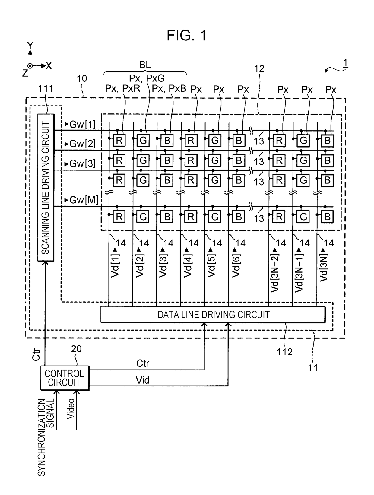
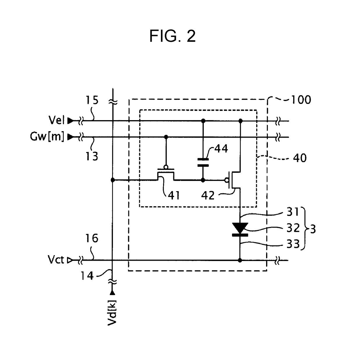
BACKGROUND1. Technical Field[0001]The present invention relates to an electro-optical device and an electronic apparatus.2. Related Art[0002]In recent years, various types of electro-optical devices for displaying an image with pixels each pixel having a light emitting element such as a silicon organic light emitting diode (OLED) element and a driving transistor for supplying a current to the light emitting element are proposed. In such an electro-optical device, generally, one display unit is formed with a pixel block configured with a plurality of pixels. For example, it is possible to display a full color image by forming one display unit with a pixel block including a pixel for displaying red (hereinafter, written as R), a pixel for displaying green (hereinafter, written as G), and a pixel for displaying blue (hereinafter, written as B).[0003]In the electro-optical device capable of displaying a full color image, in order to realize desired white brightness and color coordinates...

Claims


Application Information

Patent Timeline
Patent Type & Authority Applications(United States)
IPC IPC(8): H01L27/32
CPCH01L27/322H01L27/3272H10K59/352H10K59/38H10K59/8792H10K50/86H10K50/865H10K59/126
Inventor OTA, HITOSHI
Owner SEIKO EPSON CORP
Learn More