Method of manufacturing printed circuit board

a technology of printed circuit boards and manufacturing methods, applied in the direction of waveguides, waveguide type devices, high frequency circuit adaptations, etc., to achieve the effects of reducing the dielectric constant of the insulating resin layer, excellent productivity and reliability, and reducing transmission loss

Active Publication Date: 2019-01-24
NIPPON MEKTRON LTD
View PDF4 Cites 0 Cited by
  • Summary
  • Abstract
  • Description
  • Claims
  • Application Information

AI Technical Summary

Benefits of technology

[0020]The printed circuit board of the present invention includes the insulating resin layer having a void. The void provided to the insulating resin layer communicates with the outside of the printed circuit board. Accordingly, gas or the like enclosed in the void can flow outward, if it expands in the heating processes such as reflow process during manufacturing of the circuit board, or under changes in pressure during transportation, or under changes in ambient temperature during use. In these cases, the printed circuit board of the present invention is therefore prevented from being deformed or broken.
[0021]The printed circuit board of the present invention is excellent in the productivity and reliability, from the viewpoint of that it includes the insulating resin layer having the void. The printed circuit board of the present invention includes the insulating resin layer having the void. The printed circuit board of the present invention can, therefore, reduce the dielectric constant of the insulating resin layer, without relying upon thickening of the insulating resin layer. In addition, the printed circuit board of the present invention can reduce the transmission loss under high-speed signal transmission.
[0022]The method of manufacturing a printed circuit board of the present invention can stably manufacture a printed circuit board which includes a conductor layer, an insulating resin layer, and a signal layer, the insulating resin layer having a void, and the void being communicated with a gas phase outside of the printed circuit board.

Problems solved by technology

This sort of smartphone suffers from a trade-off between portability and provision of a sufficient battery capacity.

Method used


Image

  • Method of manufacturing printed circuit board
  • Method of manufacturing printed circuit board
  • Method of manufacturing printed circuit board

Examples


first embodiment

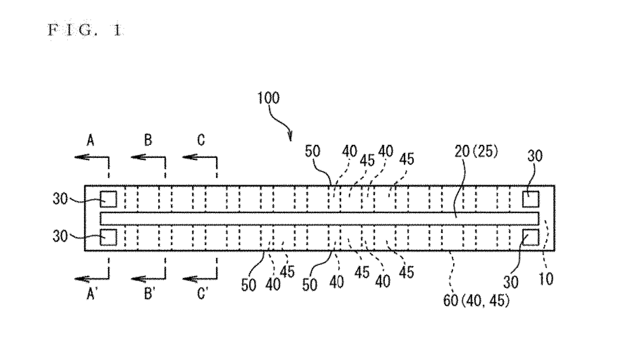
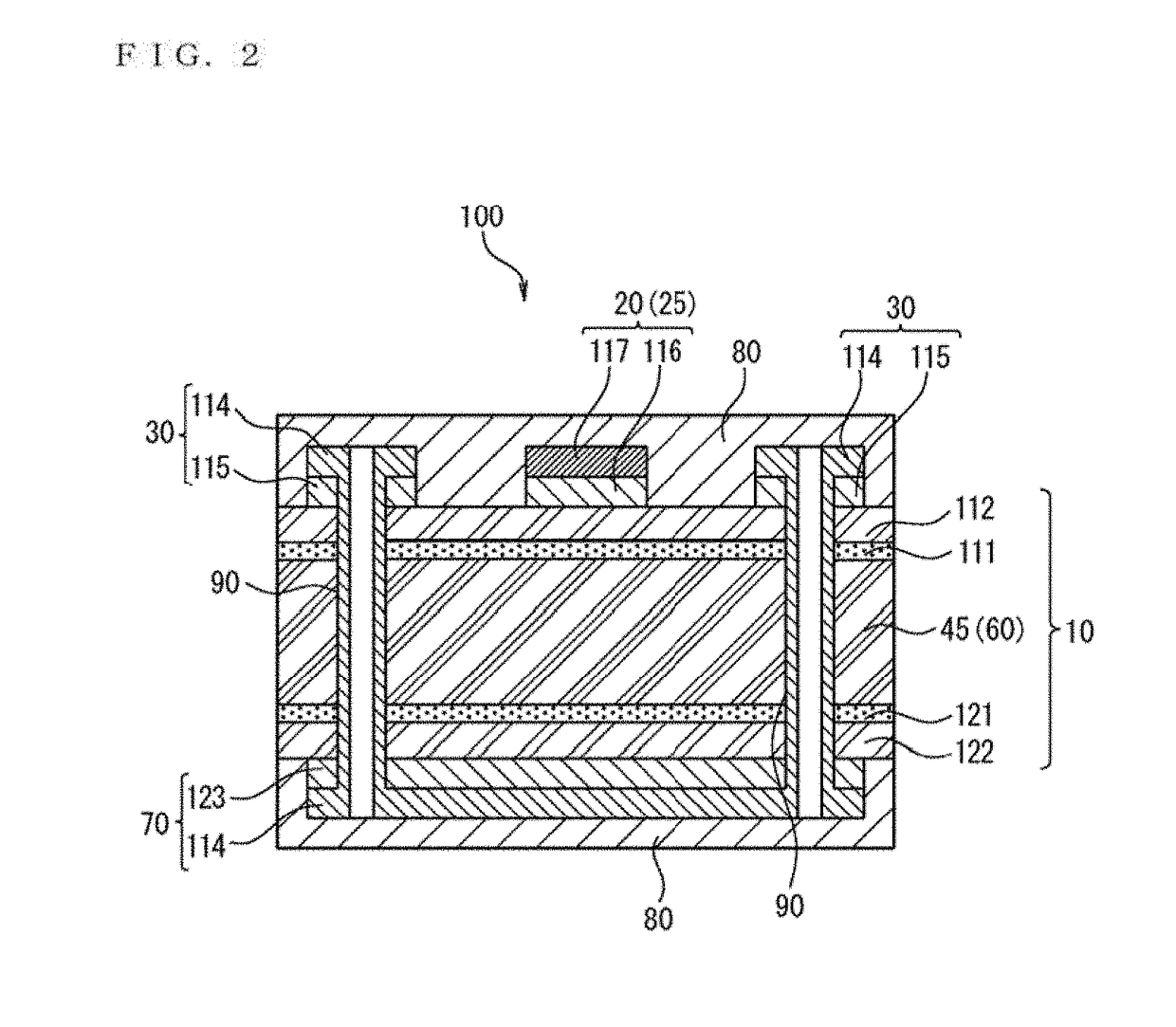
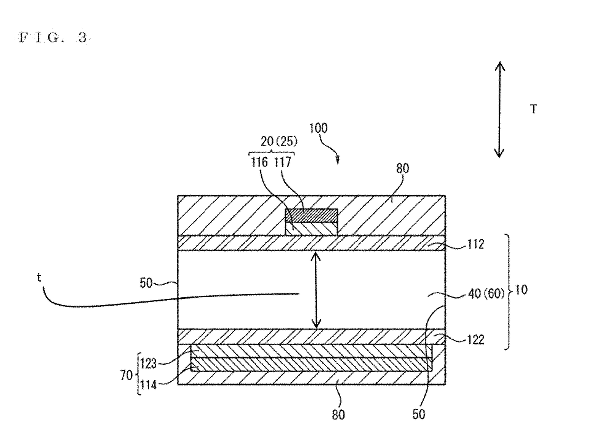
[0050]The first embodiment of the present invention will be explained referring to FIG. 1 to FIG. 5 (FIG. 5A and FIG. 5B). FIG. 1 is a plan view illustrating the printed circuit board 100 according to the first embodiment, and shows that an insulating resin layer 60 which configures an insulating layer 10 has voids 40 and insulating resin parts 45. FIG. 2 is an A-A′ cross sectional view of the printed circuit board 100 illustrated in FIG. 1. FIG. 3 is a B-B′ cross sectional view of the printed circuit board 100 illustrated in FIG. 1. FIG. 4 is a C-C′ cross sectional view of the printed circuit board 100 illustrated in FIG. 1. FIG. 5A and FIG. 5B are plan views of printed circuit boards 100a, 100b as modified examples of the first embodiment of the present invention.

[0051]As illustrated in FIG. 2, the printed circuit board 100 has a ground layer 70 as a conductor layer, a signal layer 25 having a signal line 20 provided so as to oppose the ground layer 70, and an insulating resin lay...

second embodiment

[0127]Next, a second embodiment of the present invention will be explained referring to FIG. 6 to FIG. 9. FIG. 6 is a plan view of a printed circuit board 200 of the second embodiment. FIG. 7 is a B-B′ cross sectional view of the printed circuit board 200 illustrated in FIG. 6. FIG. 8 is a C-C′ cross sectional view of the printed circuit board 200 illustrated in FIG. 6. FIG. 9 is a plan view of a printed circuit board 200a according to a modified example of the second embodiment.

[0128]The printed circuit board 200 of this embodiment is configured in the same way as the printed circuit board 100, except that the configuration of an insulating resin layer 160 is different from the configuration of the insulating resin layer 60 in the printed circuit board 100. More specifically, the pattern of formation of a void 140 and location of formation of openings 150 in the insulating resin layer 160 are different from those of the voids 40 and the openings 50 composing the insulating resin la...

third embodiment

[0148]Next, a printed circuit board 300 according a third embodiment of the present invention will be explained, referring to FIG. 10 to FIG. 14 (FIG. 14A and FIG. 14B). FIG. 10 is a plan view illustrating the printed circuit board 300 of the third embodiment. FIG. 10 is a plan view illustrating the printed circuit board 300 of the third embodiment of the present invention. FIG. 11 is an A-A′ cross sectional view of the printed circuit board 300 illustrated in FIG. 10. FIG. 12 is a B-B′ cross sectional view of the printed circuit board 300 illustrated in FIG. 10. FIG. 13 is a C-C′ cross sectional view of the printed circuit board 300 illustrated in FIG. 10. FIG. 14A is a plan view of a first insulating resin layer 311 in the third embodiment of the present invention, and FIG. 14B is a plan view of a second insulating resin layer 312 in the third embodiment of the present invention.

[0149]As illustrated in FIG. 12 and FIG. 13, the printed circuit board 300 has a ground layer 370a whic...


PUM

PropertyMeasurementUnit
flexibleaaaaaaaaaa
thicknessaaaaaaaaaa
densityaaaaaaaaaa

Abstract

The invention provides a method of manufacturing a printed circuit board. The printed circuit board (100) has a conductor layer (ground layer (70)), a signal layer (25) having a signal line (20) provided so as to oppose the conductor layer (ground layer (70)), and an insulating resin layer (60) disposed between the conductor layer (ground layer (70)) and the signal layer (25), the insulating resin layer (60) has voids in an overlapping location, in a plan view, with the signal line (20), and the voids (40) are communicated with the outside of the printed circuit board (100).

Description

CROSS-REFERENCE TO RELATED APPLICATION[0001]This application is a divisional application of U.S. application Ser. No. 14 / 441,106, filed May 6, 2015, which is a national stage application of a PCT International Application No. PCT / JP2014 / 054081 filed on Feb. 20, 2014, which claims a priority of Japanese Patent Application No. 2013-092022 filed on Apr. 25, 2013.TECHNICAL FIELD[0002]The present invention relates to a printed circuit board and a method of manufacturing a printed circuit board.BACKGROUND ART[0003]In recent years, there has been increasing trends in higher processing speed of digital circuits, and increasing needs for high-density packaging. Signal lines on printed circuit boards used for these circuits are matched in impedance so as to adjust the characteristic impedance Z0 to a constant value, in order to prevent transmission loss and degradation of communication quality. The characteristic impedance Z0 is defined by a square root of (L / C) as given by the equation (1) b...

Claims


Application Information

Patent Timeline
Patent Type & Authority Applications(United States)
IPC IPC(8): H05K1/02H05K3/00H01P3/08H05K1/03H01P11/00
CPCH05K2201/09063H05K2203/107H05K3/0044H01P3/084H01P3/082H05K1/036H01P3/08H05K3/0014H01P11/003H05K1/0216H05K1/028H05K3/0052H05K2201/0355H05K1/024Y10T29/49165
Inventor MATSUDA, FUMIHIKO
Owner NIPPON MEKTRON LTD
Why Eureka
Try Eureka