Flip chip mounting body, flip chip mounting method and flip chip mounting apparatus

a technology of flip chip and mounting body, which is applied in the field of flip chip mounting body, flip chip mounting method and flip chip mounting apparatus, can solve the problems of difficult to adapt to the current technique of forming solder bumps, difficulty in flip chip mounting of semiconductor chips, and even finer wiring, etc., to achieve excellent productivity and reliability.

Inactive Publication Date: 2010-06-08
PANASONIC CORP
View PDF18 Cites 0 Cited by
  • Summary
  • Abstract
  • Description
  • Claims
  • Application Information

AI Technical Summary

Benefits of technology

[0021]In order to solve the above-described problems, it is an object of the present invention to provide a flip chip mounted body with excellent productivity and reliability, which can mount a next-generation semiconductor chip having more than 5,000 electrode terminals on a circuit board, a flip chip mounting method and a flip chip mounted apparatus.

Problems solved by technology

However, in order to mount a next-generation semiconductor chip having more than 5,000 electrode terminals on a circuit board, it is necessary to form solder bumps that correspond to a narrow pitch of 100 μm or less, but it is difficult to adapt to it with a current technique for forming solder bumps.
As a result, the wiring becomes even finer, and the formation of the solder bumps on the area-disposed electrode terminals and the flip chip mounting of the semiconductor chip become difficult.
The plating is suitable for a narrow pitch, but has a problem in productivity due to its complicated processes.
On the other hand, the screen printing has excellent productivity, but is not suitable for narrowing a pitch because of the use of a mask.
Thereby, there also have been problems of an increase of the number of steps and an decrease of a yield.
Consequently, it is not possible to achieve solder bumps with uniform heights.
Also, in these methods, since the paste-like composition is supplied by application onto the circuit board whose surface is provided with the electrode terminals, namely, with projections or depressions, a sufficient amount of solder cannot be supplied onto the electrode terminals serving as the projections, making it difficult to achieve a desired solder bump height necessary for the flip chip mounting.
Moreover, in the flip chip mounting method described in Patent document 3, there are many problems in productivity and reliability that are to be solved as described below.
Firstly, since the electric conduction between the electrode terminals is obtained by mechanical contact via the electrically conductive particles, it is difficult to achieve a stable conductive state.
Secondarily, since a distance varies depending on an amount of the electrically conductive particles that are present between the electrode terminals of the semiconductor chip and the circuit board, the electric connection is unstable.
Thirdly, in the heating process for curing the thermosetting resin, the electrically conductive particles are scattered, which causes a decrease of a yield due to a short circuit generated thereby.
Fourthly, because of a structure where a connection part between the semiconductor chip and the circuit board is exposed and sinks into moisture or the like, and a life span and reliability of the circuit board deteriorate.

Method used


Image

  • Flip chip mounting body, flip chip mounting method and flip chip mounting apparatus
  • Flip chip mounting body, flip chip mounting method and flip chip mounting apparatus
  • Flip chip mounting body, flip chip mounting method and flip chip mounting apparatus

Examples


embodiment 1

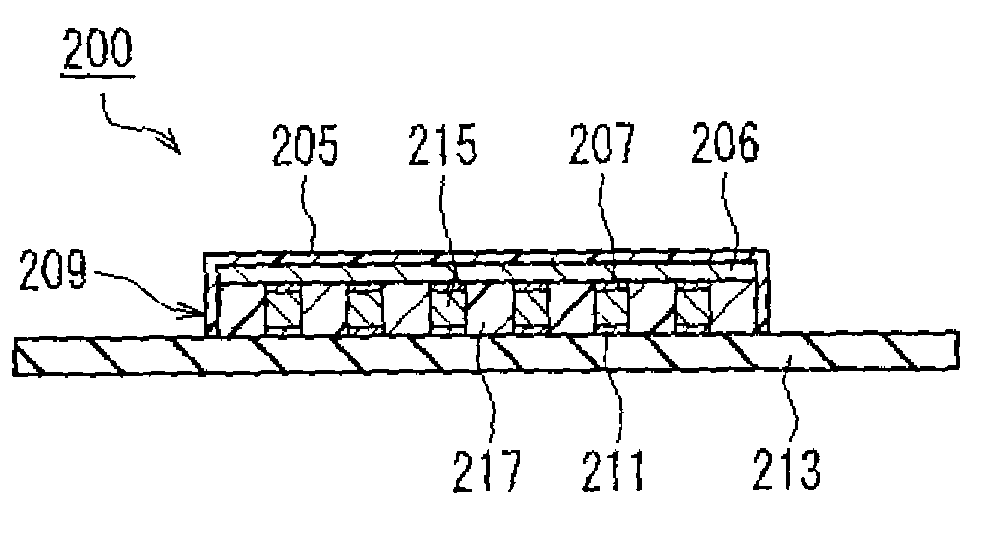
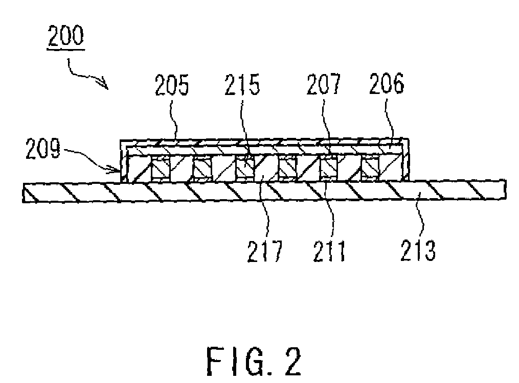
[0077]FIG. 2 is a cross-sectional view showing a flip chip mounted body according to Embodiment 1 of the present invention. In FIG. 2, a flip chip mounted body 200 according to Embodiment 1 of the present invention has a configuration where a plurality of connection terminals 211 formed on a circuit board 213 and a semiconductor chip 206 having a plurality of electrode terminals 207 that are disposed opposing the connection terminals 211 are connected electrically via a solder layer 215. Then, a porous sheet 205 that is provided on an opposite side of a formation surface of the electrode terminal 207 of the semiconductor chip 206 is folded to have a box shape 209 on the formation surface side of the electrode terminal 207 on an outer periphery of the semiconductor chip 206, and is formed so as to cover the semiconductor chip 206, whereby an end surface of the box shape 209 is in contact with the circuit board 213. Further, in a space formed by the circuit board 213 and the porous sh...

embodiment 2

[0097]FIGS. 4A to 4D are process views schematically explaining a flip chip mounted body and a flip chip mounting method according to Embodiment 2 of the present invention. It should be noted that the elements in FIGS. 4A to 4D that are the same as those in FIGS. 3A to 3E will be denoted by the same reference numerals, and the explanations thereof will be omitted.

[0098]Herein, a flip chip mounted body 300 in Embodiment 2 of the present invention adopts a mounting method that is different from that of the flip chip mounted body 250 of Embodiment 1, and has the same configuration except for this.

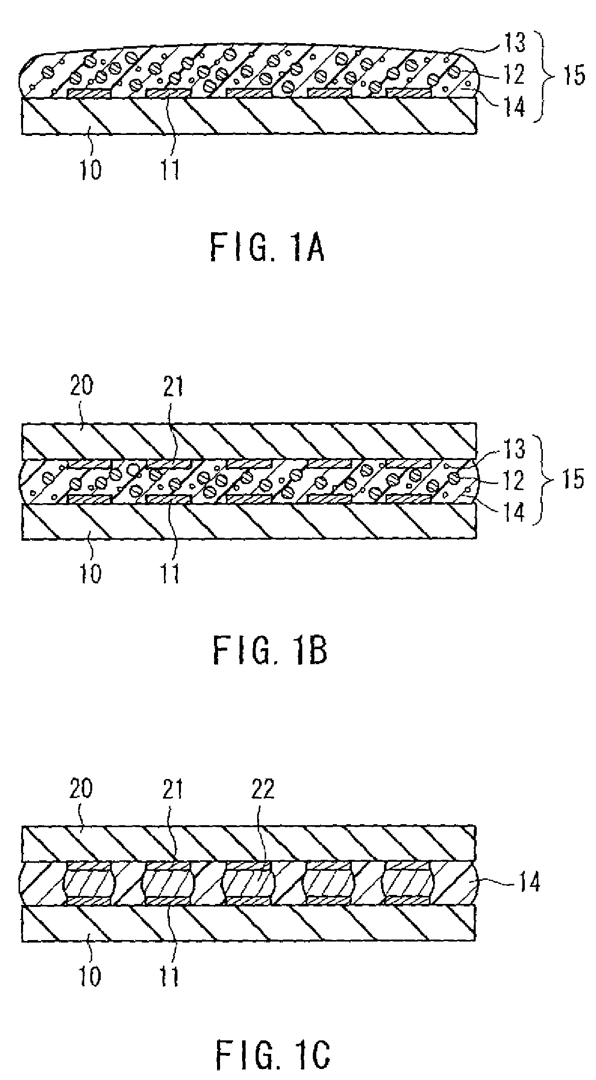
[0099]Firstly, as shown in FIG. 4A, the connection terminal 211 on the circuit board 213 and the electrode terminal 207 of the semiconductor chip 206 are disposed opposing each other in advance. Then, between the semiconductor chip 206 and the circuit board 213, the resin composition 212 containing solder particles in a paste state, a convection additive and a resin as main components is appli...

embodiment 3

[0111]FIGS. 5A to 5D are process views schematically explaining a flip chip mounted body and a flip chip mounting method according to Embodiment 3 of the present invention. It should be noted that the elements in FIGS. 5A to 5D that are the same as those in FIGS. 3A to 3E will be denoted by the same reference numerals, and the explanations thereof will be omitted.

[0112]Herein, a flip chip mounted body 400 in Embodiment 3 of the present invention is different from the flip chip mounted body 250 in Embodiment 1 in the point that the porous sheet 205 has a brim 401 and a method for mounting it, and other configurations except for these are common.

[0113]Firstly, as shown in FIG. 5A, the porous sheet 205 is deformed to have a box shape that is provided with the brim 401 by the upper mold 201 and the lower mold 208 in advance.

[0114]The below description will provide an example where the brim 401 is provided by folding the edge of the porous sheet 205 having the box shape, but the present ...


PUM


Abstract

The flip chip mounted body of the present invention includes: a circuit board (213) having a plurality of connection terminals (211); a semiconductor chip (206) having a plurality of electrode terminals (207) that are disposed opposing the connection terminals (211); and a porous sheet (205) having a box shape that is provided on an opposite side of a formation surface of the electrode terminal (207) of the semiconductor chip (206), is folded on an outer periphery of the semiconductor chip (206) on the formation surface side of the electrode terminal (207) and is in contact with the circuit board (213), wherein the connection terminal (211) of the circuit board (213) and the electrode terminal (207) of the semiconductor chip (206) are connected electrically via a solder layer (215), and the circuit board (213) and the semiconductor chip (206) are fixed by a resin (217). Thereby, the flip chip mounted body with excellent productivity and reliability that can mount the semiconductor chip on the circuit board, and a method and an apparatus for mounting the flip chip mounted body are provided.

Description

TECHNICAL FIELD[0001]The present invention relates to a flip chip mounting method for mounting a semiconductor chip on a circuit board. In particular, the present invention relates to a flip chip mounted body that is adaptable to a semiconductor chip with a narrower pitch and has high productivity and excellent reliability of connection, a method for mounting the same, and a flip chip mounted apparatus.BACKGROUND ART[0002]In recent years, with a trend toward a higher density and a higher degree of integration for a semiconductor integrated circuit (hereinafter, abbreviated as a “semiconductor”) chip used for electronic equipment, the number of pins of electrode terminals of a semiconductor chip has been increased and the pitch thereof has been decreased rapidly. For mounting these semiconductor chips on circuit boards, flip chip mounting is used widely in order to decrease a wiring delay.[0003]In this flip chip mounting, solder bumps generally are formed on electrode terminals of th...

Claims


Application Information

Patent Timeline
Patent Type & Authority Patents(United States)
IPC IPC(8): H01L23/04H01L23/06
CPCH01L21/563H01L24/75H01L24/81H01L24/83H01L2224/83874H01L24/29H01L24/32H01L2224/16225H01L2224/73203H01L2224/75H01L2224/75251H01L2224/83007H01L2224/83097H01L2224/83192H01L2224/83815H01L2224/8388H01L2224/83888H01L2224/9201H01L2924/01009H01L2924/01011H01L2924/01013H01L2924/01027H01L2924/01033H01L2924/01056H01L2924/01078H01L2924/01082H01L2924/14H01L2924/3025H01L2224/2919H01L2924/01006H01L2924/0105H01L2924/014H01L2924/0665H01L24/16H01L2224/29111H01L2224/73204H01L2224/32225H01L2924/0132H01L2924/00H01L2924/0695H01L2224/05568H01L2224/05573H01L2924/00014H01L2924/181H01L2224/05599
Inventor NAKATANI, SEIICHIKITAE, TAKASHIYAMASHITA, YOSHIHISAICHIRYU, TAKASHIKARASHIMA, SEIJI
Owner PANASONIC CORP
Why Eureka
Try Eureka