Anisotropic conductive film

Pending Publication Date: 2019-01-31
DEXERIALS CORP
View PDF2 Cites 3 Cited by
  • Summary
  • Abstract
  • Description
  • Claims
  • Application Information

AI Technical Summary

Benefits of technology

[0015]With the anisotropic conductive film of the present invention, the individual conductive particles are not arranged in a simple lattice form, and repeating units of conductive particles having a specific particle arrangement are disposed repeatedly. Therefore, sparse and dense regions of conductive particles can be formed on the film, and thereby increases in the number density of conductive particles can be suppressed over the entire anisotropic conductive film. Accordingly, increases in production cost associated with increases in the number density of conductive particles can be suppressed. In addition, when the number density of conductive particles increases, the thrust required for the pressing jig at the time of anisotropic conductive connection typically also increases. However, with the anisotropic conductive film of the present invention, increases in the thrust required for the pressing jig at the time of anisotropic conductive connecti

Problems solved by technology

Therefore, when the bumps have a narrow pitch, the distance between the conductive particles needs to be narrowed, which makes it difficult to avoid shorting.
In addition, the number density of the conductive particles increases, and the production cost of the anisotropic conductive film also increases.
On the other hand, when the distance between conductive particles is not narrowe

Method used


Image

  • Anisotropic conductive film
  • Anisotropic conductive film
  • Anisotropic conductive film

Examples


Example

Experimental Examples 1 to 8

Production of Anisotropic Conductive Film

[0113]For the anisotropic conductive films to be used in COG connection, the effects of the resin composition of the insulating resin binder and the disposition of the conductive particles on the film forming capacity and conduction properties were investigated as follows.

[0114]First, resin compositions forming insulating resin binders and insulating adhesive layers were respectively prepared with the formulas shown in Table 1. In this case, the minimum melt viscosity of the resin composition was adjusted by the preparation conditions of the insulating resin composition. The resin composition forming the insulating resin binder was applied to a PET film with a film thickness of 50 μm using a bar coater, and this was dried for 5 minutes in an oven at 80° C. to form an insulating resin binder layer with the thickness La shown in Table 2 on the PET film. Similarly, an insulating adhesive layer was formed on the PET fi...

Example

[0138]It can be seen from Table 2 that in Experimental Example 4 in which the minimum melt viscosity of the insulating resin binder was 800 Pa·s, it is difficult to form a film having concavities in the insulating resin binder in the vicinity of the conductive particles. On the other hand, it can be seen that in the experimental examples in which the minimum melt viscosity of the insulating resin binder was 1500 Pa·s or higher, convex portions can be formed in the vicinity of the conductive particles of the insulating resin binder by adjusting the conditions at the time of the embedding of the conductive particles, and that the resulting anisotropic conductive films have good conduction properties for COG. In addition, it can be seen that in Experimental Examples 1 to 7 in which the number density of the conductive particles is lower than in Experimental Example 8, which has a hexagonal lattice arrangement, anisotropically conductive connection can be performed at a lower pressure.

(...

Example

Experimental Examples 9 to 16

Production of Anisotropic Conductive Film

[0146]For the anisotropic conductive films to be used in FOG connection, the effects of the resin composition of the insulating resin binder and the disposition of the conductive particles on the film forming capacity and conduction properties were investigated as follows.

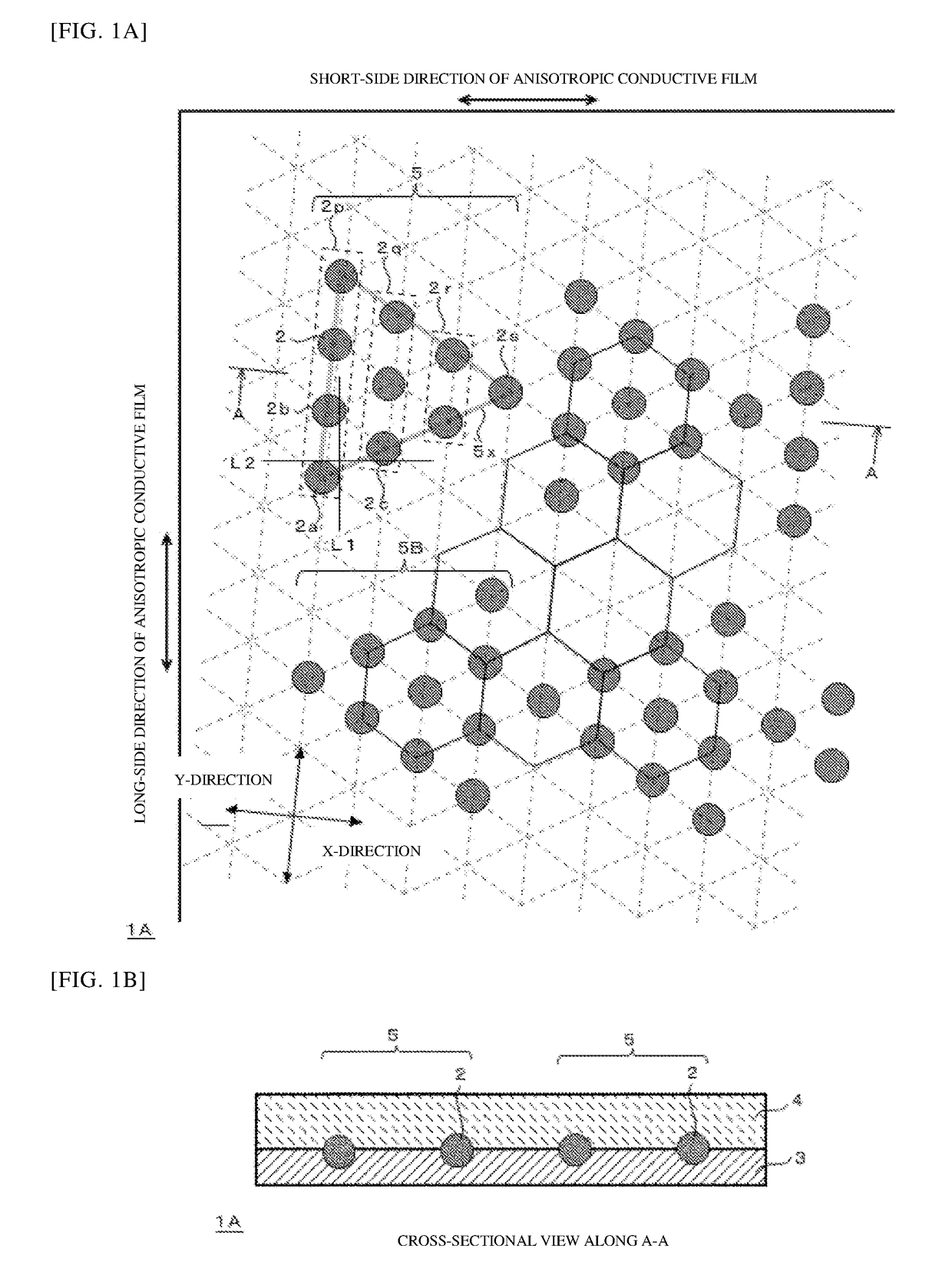
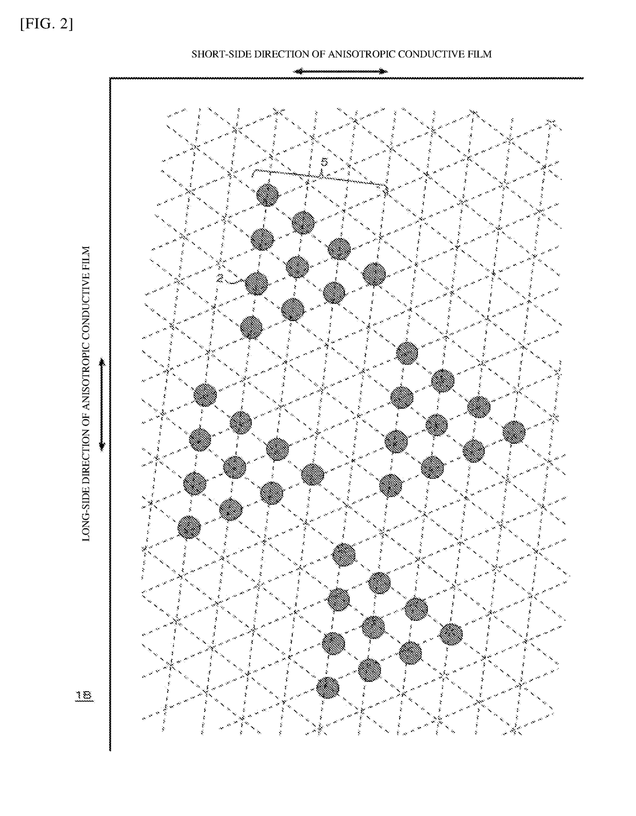
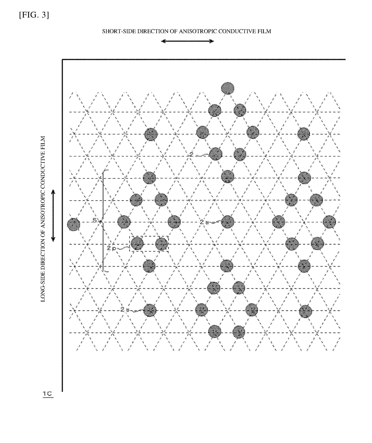
[0147]Specifically, resin compositions for forming insulating resin binders and insulating adhesive layers were prepared with the formulas shown in Table 3, and anisotropic conductive films were produced in the same manner as in Experimental Example 1 using these resin compositions. The disposition of the conductive particles and the center distance of the closest particles are shown in Table 4. In Experimental Example 16, the disposition of the conductive particles was a hexagonal lattice arrangement (number density: 15000 particles / mm2), and one lattice axis thereof was inclined by 15° with respect to the long-side direction of the anisotropic ...


PUM

PropertyMeasurementUnit
Lattice constantaaaaaaaaaa
Densityaaaaaaaaaa
Electrical conductoraaaaaaaaaa

Abstract

An anisotropic conductive film capable of accommodating bumps with a narrow pitch and reducing the number density of conductive particles. In an anisotropic conductive film, conductive particles are disposed in an insulating resin binder as follows. Specifically, the conductive particles are rows of conductive particles arranged in single rows with spacing therebetween; and repeating units of conductive particles formed by juxtaposition of different numbers of conductive particles are disposed repeatedly over the entire surface of the anisotropic conductive film.

Description

TECHNICAL FIELD[0001]The present invention relates to an anisotropic conductive film.BACKGROUND ART[0002]Anisotropic conductive films in which conductive particles are dispersed in an insulating resin binder are widely used when mounting electronic components such as IC chips to wiring boards or the like. In an anisotropic conductive film, there is a strong demand to increase the capacity to capture conductive particles on bumps and to avoid shorting between adjacent bumps by narrowing the pitch of bumps, which accompany the high-density mounting of electronic components.[0003]To meet such a demand, it has been proposed to use a lattice-like arrangement for the disposition of conductive particles in an anisotropic conductive film, to make the arrangement axis inclined with respect to the long-side direction of the anisotropic conductive film, and to increase the distance between conductive particles by a prescribed ratio in this case (Patent Documents 1 and 2). It has also been prop...

Claims


Application Information

Patent Timeline
IPC IPC(8): H01L23/00H01B1/22
CPCH01L24/73H01L24/14H01L24/29H01L24/32H01L24/83H01B1/22H01L2224/73104H01L2224/1412H01L2224/2929H01L2224/32225H01L2224/83203H01R11/01H01R43/00B32B5/16H01L24/27B32B27/20C09J9/02C09J7/10C09J2301/304C09J2301/314H01L2224/73204H01L2224/83851B32B2260/046H01L2224/16225H01L2224/29355C08K2201/001H01L2224/27436H01L2224/29339H01L2224/83101H01L2924/14C09J2203/326B32B2260/025H01L2924/00012H01L2224/29082H01L2224/29364H01L2224/2939H01L2224/29455H01L2224/81903H01L2224/2731H01L2924/15788C09J2301/408H01L24/16H01L24/81H01L2224/2919H01L2924/00014H01L2224/29344H01L2224/29499H01L2224/13099H01L2924/00H01B5/16
Inventor TSUKAO, REIJIAKUTSU, YASUSHI
Owner DEXERIALS CORP
Why Eureka
Try Eureka